The fall detector is suitable for elderly people and children with poor self-care ability and self-protection ability. It senses the change of body posture by measuring the acceleration of three individuals wearing the instrument in the three orthogonal directions during exercise. Alert and post as needed.
The fall detector consists of an acceleration sensor, a data processing module, a power supply, and a communication module. The sensor measures the acceleration vector of the object; the processor module is responsible for collecting the data of the acceleration sensor, analyzing and determining the body posture of the object and controlling the release of the alarm and alarm information; the power module is responsible for providing power supply to the entire system; the communication module is responsible for passing the alarm information A certain agreement is issued.
Key technology
Establishment of human motion model
During the attitude transition, gravity will become the main factor affecting this movement process. During the fall, the three vectors of acceleration, velocity and displacement of the object changed.
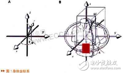
As shown in Fig. 1, the Cartesian coordinate system is established, and the X, Y, and Z axes are orthogonal to each other, and the vector changes in any spatial direction can be decomposed into component changes in the three directions of X, Y, and Z. When the user correctly wears the fall detector and is in a static or horizontal uniform motion state, the acceleration in the Z-axis direction is the gravitational acceleration (g), and the acceleration in the other two directions is 0. When the wearer falls, it can be found that only the initial state and the final state are considered. Ideally, the Z-axis component changes from the maximum value (1g) to 0, and the X or Y-axis component changes from 0 to the maximum (1g). ), specifically whether the X-axis or the Y-axis changes, is determined by the posture of the wearer after the fall--the flat is the X-axis change, and the side is the Y-axis change. If the body posture is between the lying and lying sides, the acceleration components of the X and Y axes will satisfy sqrt{x^{2}+y^{2}}=1g (this vector sum is 0 when standing) It is still possible to obtain a different acceleration distribution from standing by calculation and analysis.
However, in the actual situation, it is difficult to distinguish the cause of the collapse posture based on the change of the acceleration component, and it is prone to many false positives (detection of a fall without actually falling) or false negatives (a fall is not detected and a fall actually occurs). Therefore, an algorithm is needed for further improvement. In general, the false positive situation can be screened by analyzing the acceleration of the acceleration in the time domain and the two integrals to find the displacement, and the wearer's body posture changes are analyzed in all aspects; In addition, the wearer needs to participate independently in order to effectively improve the detection efficiency. Therefore, establishing the motion model of the human fall process and extracting the characteristic parameters of the body posture change during the fall are the key to accurately detecting the fall and issuing the alarm information.
Wireless communication and spatial positioning information acquisition
The fall alarm must be delivered to the rescue center in time to ensure the effectiveness of the rescue. The timely release of the alarm message contains two meanings: one is that the alarm information will not be affected by the action and location of the fall detector wearer; Second, the issued alarm information should include the geographical location of the wearer's fall, so as to ensure that the faller is effectively rescued.
The use of wireless communication to release fall alarm information is very suitable for wearers who are free to move. Wireless communication technology is also very applicable from the perspective of technology maturity and operating cost. From the technical realization and cost considerations, the choice of CDMA communication mode is more suitable for the realization of the design of the fall detector.
System design
demand analysis
Body posture monitoring
The wearer's body posture is calculated by the corresponding algorithm through the measured values ​​of the three-axis acceleration sensor. When a fall action occurs, the MCU interrupt processing can be triggered.
Alarm control mechanism
The user can choose whether to alarm according to his or her physical condition. When the user has no control over his behavior, the product should be able to guarantee the automatic implementation of the alarm.
Pedometer
In the general wearing process, users can use this function to provide quantitative reference information for their walking fitness activities.
Spatial positioning
When implementing the fall alarm, the receiver of the alarm information should be provided with the spatial location information of the alarm location to ensure that the effective rescue arrives in time.
Wireless communication
The alarm and positioning information can be transmitted wirelessly to the relevant personnel.
Power supply using lithium battery
Some information shows the use of the LCD screen
System architecture design
According to the demand analysis of the fall detector, the specific implementation design uses the architecture shown in Figure 2. The architecture is based on the high-performance, low-power MCU--MC9S08QG8. By acquiring the acquisition information of the acceleration sensor, it analyzes and calculates the fall detection and alarm functions.
hardware design
The hardware design is built around the MCU. The product uses the MC9S08QG8 chip. How to make full use of the chip resources and properly complete the task processing of the product is the key to the design. Referring to the system structure framework, according to the functional module division, the hardware design of the system is described in detail as follows:
Acceleration acquisition circuit
Acceleration acquisition uses MMA7260QT, the chip output is an analog signal, and A/D conversion is required before data processing can be performed. The PA pin of the MC9S08QG8 chip is a multiplexed channel, which can be set to I/O, keyboard interrupt or A/D sampling channel as needed. This design will use the A/D module inside the MC9S08QG8 chip to realize analog-to-digital conversion. In the specific implementation, PA0, PA1 and PA2 are used as the acquisition channels of the three-axis acceleration, and Xout (PIN15), Yout (Pin14) and Zout (Pin13) of the MMA7260QT. Connected, the control clock of A/D sampling is completed by software configuration MC9S08QG8 corresponding control register.
MCU peripheral circuit
In this design, the MCU peripheral circuit consists of three parts: power supply and clock, data buffer and key circuit, which are described separately below.
Power and clock
Functional components include MCU, LCD, buttons, acquisition, data storage and communication. According to the data sheet of the selected device, the power supply requirements of each component are shown in Figure 3.
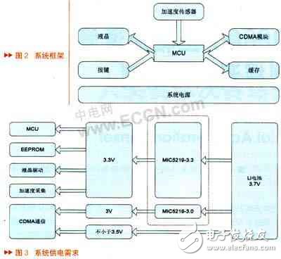
As can be seen from the figure, the entire system design requires three power supply parameters, namely 3V, 3.3V and 3.7V. Among them, the main digital circuit part--including the MCU and its peripheral circuit part requires 3.3V working voltage; and in the wireless communication module, the 3V supply voltage is required for reading the incoming SIM card part of the circuit, and the CDMA RF part working voltage requirement Not less than 3.5V.
In the actual design, the output voltage is 3.7V. Because it can meet the working requirements of the CDMA RF module, the output power of the Li battery is directly used. The working voltage of the SIM card information reading circuit of China Unicom is 3V, and the design uses MICREL. The MIC5219-3.0 chip performs voltage conversion work; the other digital circuit part operates at 3.3V. The MICREL MIC5219-3.3 chip is used in the design to achieve this conversion. See the dotted box in Figure 3.
The MC9S08QG8 has its own clock module (ICS). In order to reduce power consumption and simplify the design, the system sets the corresponding control register through software to realize the stable operation of the system clock. Therefore, it does not need to be considered too much in the hardware circuit design.
Memory
A valid data cache requires a memory depth of at least 320 points (1920 bytes). In this design, HoLTEk's HT24LC16 serial EEPROM is used as the data buffer. The chip adopts I2C communication interface, the storage depth is 2K bytes, and the data read and write speed is in the subtle level, which can meet the requirements of real-time data writing. After the data is full, the MCU automatically resets the address and overwrites the new data from the first address.
Since the MC9S08QG8 is equipped with an I2C control module, it is only necessary to connect the corresponding pin of the module to the EEPROM--using PB6 (Pin5) and PB7 (Pin6) to connect to the EEPROM.
Button circuit
Alarm acknowledgement, alarm cancellation, pedometer start, pedometer pause, count clear, and receiver number setting in wireless communication require the fall detector to have an interface for user input, which is implemented using buttons. The connection and use of the buttons is relatively simple, and the input and output pins of the MCU can be directly used. The design adopts Pin1 and Pin13.
LCD
The design adopts a 5-digit 7-segment LCD screen, and the pedometer display count and the alarm receiver's telephone number input are provided to the user for confirmation through the LCD screen. There are 24 control pins on the LCD screen. Since the LCD control of all the pin seats of the MCU can not meet the working requirements, the Holtek HT1621B liquid crystal driver chip is used in this design to manage and drive the display data from the MCU to the LCD screen. In addition, the HT1621B chip also has buzzer control and drive capability. In this design, the integrated buzzer as a live alarm prompt will help to improve the pertinence and accuracy of the fall detector alarm, which will pass the BZ tube in the HT1621B. A buzzer is connected to the foot.
The HT1621B is an I2C interface that allows the MCU to transfer instructions and data to the chip through the internal I2C control block. Since the EEPROM used in this system also uses the I2C interface, data transmission and control instructions for different devices will be implemented by address selection.
Communication module
This design uses AnyData's DTGS-800b OEM module. The module complies with CDMA: IS-95 A/B, IS-98A, IS-126, IS-637A, IS-707A, and IS-2000. It can provide data communication speeds up to 153.6K, and the operating voltage is 3.6V~ 4.4V, size 53*33*2.7mm, total weight 15g, providing external communication interface including RS-232s, Digital/Analog Audios, LCD, Keypad, Ringer External Reset Control, R-UIM, MP3, MIDI, GPIOs And USB. In addition, the module can send and receive text messages, integrate GpsOne technology, and obtain geolocation information without adding other components, and the manufacturer's technical support is perfect, and its various functional configurations are very suitable for the description of the fall detector.
In the specific implementation, the CDMA module requires a SIM card to be connected to the network, and the functions of the module can be called by the MCU through the RS232 interface in the form of an AT command. The design of the communication module in this design is shown in Figure 4.
The SCI peripheral interface of the MC9S08QG8 is connected to the RS232 port of the DTGS-800b after being converted by TTL-RS232 to send AT commands to the module. Since the module requires the RS232 interface of the 7-signal, and the MCU's own SCI does not provide such communication mode, the I/O port is used in the system design to simulate other control signals: CTS, RFR and DTR. The DTGS-800b module is connected to the SIM card through the SIM card reading circuit, and the internal self-contained processor reads the SIM card information as needed to complete the CDMA network access and exchange of communication information.
Port assignment
Because this design uses MC9S08QG8 microcontroller to provide only up to 14 I/O ports, it can not meet the requirements of controlling the number of signals running in the whole system. Therefore, when the specific design is carried out, the use and allocation of each pin are specially deployed. As shown in Figure 5.
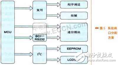
Two ports are required for program debugging and burning, but after debugging and programming, these two ports can be used as standard I/O, so one I/O (Pin1) is used as the input of the button in the design. The multiplexing of the ports is implemented.
Communication requirements between CDMA components and MCUs
Via 7 signal RS232 interface, while MC9S08QG8
The SCI module has only two signals, TXD and RXD. In the design, standard I/O is used to implement other required signals through software simulation, including DTR, CTS, and RFR.
The EEPROM and LCD driver components are accessed using the I2C interface. In this design, the I2C module of the MC9S08QG8 is used for hardware control, and the switching between different components is realized by address selection.
software design
Software design is the key to the specific implementation of the system's functions. In the software design of the fall detector, the processing content caused by the solid line system function is more. In order to better utilize and allocate the resources of the MCU, a design method combining transaction processing and state machine is adopted.
Transaction processing and state machine
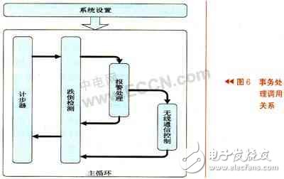
According to the design requirements of the fall detector, the system must have functions such as pedometer, fall detection, alarm processing, system setting and wireless communication control.
The transaction processing method draws on the thread concept in the operating system. First, the operation performed by each transaction is clear, the priority, interrelationship, and resource requirements of each operation are determined. Then, the startup mechanism of various operations is set in the main loop. Generally, these things are in the main loop. Implemented in parallel. The call relationship of the fall probe transaction is shown in Figure 6.
For the implementation of certain transaction processing, a state machine approach is adopted in the software design to ensure that the entire task can be implemented smoothly and correctly.
System settings
The system settings mainly perform some initialization operations and setting operations of system information that requires the user to confirm.
The system initialization work is mainly completed by the MCU, including the setting of various configuration registers, the liquid crystal initialization instruction and the setting of the storage buffer. The initialization work will ensure that all functional components of the system can be started normally after power-on.
MCU initialization --MCU_Init( ):
The startup of the MCU and the management of each functional peripheral (Peripheral) are implemented by setting the corresponding control registers:
Clock: The MCU works with an internal clock and is implemented by setting the ICS control register.
Port: According to the system port allocation scheme, combined with the relevant peripherals - I2C, SCI control register implementation;
I2C controller: transmission rate, address selection setting;
SCI controller: Baud rate setting.
LCD initialization - LCD_Init ():
The liquid crystal display is initialized by initializing the liquid crystal drive control chip HT1621B by an instruction.
Storage buffer initialization --RT_Data, Word_Base[ ]:
The MC9S08QG8 integrates 512 bytes of RAM internally to meet the needs of the program. During the operation of the fall detector, the MCU continuously collects the data of the acceleration sensor and processes it, so a buffer area is pre-opened for data analysis. Similarly, when using CDMA to issue alarm information, the text content of the alarm message needs to be pre-set during software design and called by the pointer when needed.
The setting of the system information that requires the user to confirm is that the receiver of the fall detector alarm information can be set by the user according to the actual situation, such as the mobile phone of the relative or the fixed landline of the emergency center (requires the ability to receive the short message) . The user can press the LCD to input the number of the recipient, and the user can modify the recipient number if necessary.
Key Function
The button function is separately proposed in the software design because the system is limited by the number of MCU ports, and it is not possible to arrange enough ports for keyboard scanning according to the pre-designed human-computer interaction requirements. In this design, it is finally determined that two buttons are used, and the function setting and usage of the buttons are designed as follows.
"Alam" button (starts alarm receiver number entry, manual alarm):
In the normal working mode of the fall detector, long press (more than 2 seconds) "Alam" button to activate the alarm information release function, which is suitable for other emergencies except for the fall situation;
In the normal working mode of the fall detector, press the “Alam†button, the fall detector enters the state of setting the alarm receiver number, and the “Alter†button is used to realize the number input;
When the fall detector enters the alarm processing state (buzzer beep), press the “Alam†button to directly issue the alarm message, and then turn off the buzzer;
“Alter†button (the pedometer starts, pauses, clears, cancels the alarm, sets the alarm receiver number):
In the normal working mode of the fall detector, press the “Alter†button to switch between the pedometer start, pause and clear functions;
When the fall detector enters the alarm receiver number input state, the "Alter" key performs the operation of adding the number of the liquid crystal display, and the number is cycled from 0-9;
When the fall detector enters the alarm processing state (buzzer beep), press the “Alter†button to cancel the alarm and then turn off the buzzer.
Pedometer
The MCU always analyzes the wearer's body posture information, so the wearer's walking motion analysis can be output as an auxiliary result, so that the fall detector also has the function of the pedometer.
Referring to Figure 1, during the ideal walking process, both the X-axis and the Z-axis should be able to detect periodic changes in acceleration - the X-axis is caused by the forward motion and the Z-axis is caused by the ups and downs of the body. Sexual changes can provide a basis for the analysis of walking movements. Since the body's corresponding shaking with the stepping motion also causes the acceleration sensor to output in three orthogonal coordinate axes during actual use, an appropriate acceleration threshold should be set when designing the detection algorithm. Only output exceeding a certain amplitude is considered to be caused by the step movement, avoiding various artifacts introduced due to normal body sway. The software flow of the pedometer implementation is shown in Figure 7.
Fall detection
After a fall that is dangerous or may have a more serious consequence, the human body is usually in a horizontal state, so for this type of fall, the fall detector is required to detect and implement an alarm handling mechanism. For other more complicated fall processes, it is necessary to cooperate with the alarm mechanism to achieve accurate triggering of fall detection and dangerous alarms. The algorithm state machine for fall detection is shown in Figure 8.
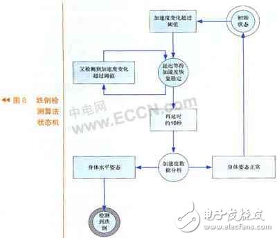
The fall detection algorithm is described as follows:
1) The main loop waits to monitor the Z-axis acceleration change. If the threshold is exceeded, the next step is entered;
2) Wait for the acceleration to return to the normal range and proceed to the next step;
3) Set the delay for another 10 seconds, waiting for the wearer to be in a stable state;
4) Data analysis, if the wearer's body level is found, it is considered that a fall condition occurs, and an alarm is triggered.
Alarm processing
In this design, a fall detection algorithm combined with multiple alarm modes is used. When the fall detector detects a fall, the system must be able to release the alarm information accurately and correctly to ensure that the faller gets help. There are many types of falls. In some cases, the detected "fall" is a conscious act -- or not a fall -- a false positive. In addition, sometimes the faller still maintains a certain ability to act, in order to get help as soon as possible, Some action can be taken; there is also a situation in which the fall has serious consequences and the faller is unable to act.
For the above mentioned cases, the software design of the alarm processing will be treated differently:
After detecting the fall, the system starts the 30S countdown timer and turns on the buzzer, which sounds once every 3S. If no input is received, the system automatically issues an alarm message after the end of 30S;
After entering the 30S countdown, the buzzer "beep", the system can respond to user input, the two buttons of the fall detector are set to "manual alarm" and "cancel (alarm)" respectively, if the user presses the "manual alarm" button , the system issues an alarm message;
If the user presses the "Cancel" button, the system turns off the 30S countdown and buzzer, and returns to the pedometer and fall detection status without any processing.
Communication control
The alarm information is sent to the receiver through CDMA SMS. The fall detector uses the DTGS-800b CDMA module. Communication control is a routine that enables it to work normally. The DTGS-800b CDMA module provides an RS232 interface, and the MCU can control the communication process through AT commands as needed. The specific communication routines should include the following according to the design requirements:
Start the CDMA module --Comm_Start( );
Start GpsOne? Service--Gps_Start( );
Obtain GPS spatial positioning information--Gps_PosiTIon( );
Send a short message alert -- Send_SMS( ).
Since the communication routine involves a small number of states, it is basically performed in the above order, so the program structure is relatively simple, and will not be described here.
in conclusion
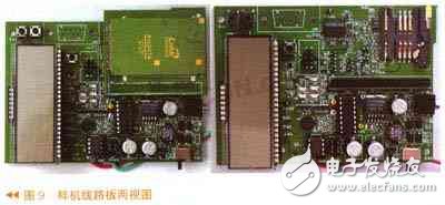
The falling detector prototype circuit board designed according to the above scheme is shown in Fig. 9. The left picture shows the line with CDMA module, and the right picture shows the line without CDMA module. It can be seen that the SIM card circuit is read below. After power-on, the function modules of the circuit board work normally, and can complete acceleration acquisition, EEPROM data storage and fall alarm SMS sending (including automatic, manual and cancel modes), and the button LCD can be normal.
Put the Samsung in the leather case , it will protect your phone .We sell Samsung Phone Case,hot selling Samsung phone case,leather phone cases,etc.
We employ the most creative designers and tech brilliant engineers to make the best cases. We believe our high-quality products with competitive prices will satisfy your needs.
The productive process :
Make the Products Mould –Cutting the fabric –Do the half products – Finish products – Cleaning –QC- Package – Shippment .
For Samsung case,Samsung case cover,hot selling Samsung phone case,leather phone cases
Ysure Leather case 24/7 Support : 86 13430343455 , https://www.ysurecase.com