Timing performance is one of the most important metrics for FPGA design. There are many root causes for poor timing performance, but the direct causes can be divided into three categories: poor layout, too many logical levels, and excessive signal fanout. The timing analysis example is used to locate the cause and give the corresponding solution.
1. Poor layout and solutionThe timing report shown in Figure 5-13, with an additional surrounding constraint of 3ns, a real cycle of 3.027ns, a logic time of only 0.869ns, and a routing delay of 2.203ns, is clearly due to poor layout.
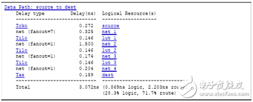
Figure 5-13 Schematic diagram of the timing report with poor layout
The corresponding solutions are:
1) Effort level to adjust the layout in the ISE layout tool;
2) Use the extra effort or MPPR option of the place and route tool;
3) If the user is familiar with the regional constraints, use the Floorplanner Relative Area Constraint (RLOC) to re-plan the design.
In FPGA design, the higher the number of logic levels, the higher the utilization of resources, but the greater the impact on the design operating frequency. In the example shown in Figure 5-5, the additional surrounding constraint is 3ns, the actual period is 3.205ns, and the logic time is 1.307ns, which has already had a certain impact on the actual performance of the design. In this case, there is no improvement in the ISE implementation tool, and the code must be modified to improve performance. The corresponding solutions are:
1) Using pipeline technology, insert registers in combinatorial logic to simplify the original logic structure;
2) Check if the path is a multi-cycle path, and if so, add a corresponding multi-cycle constraint;
3) Have good coding habits, don't nest if statements or if, case statements, and try to replace if statements with case statements.
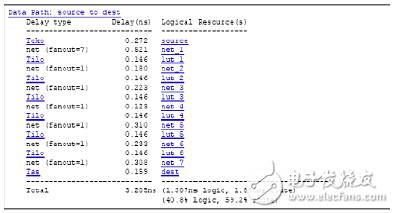
Figure 5-14 Schematic diagram of timing report with too many logical levels
3. Signal fanout is too high and the solutionHigh fanouts can cause signal transmission paths to be too long, reducing timing performance. As shown in Figure 5-15, the additional period constraint is 3ns, and the actual period is 3.927ns. The fanout of the network cable is as high as 187, resulting in a wiring delay of 3.003ns, accounting for 77.64% of the actual delay. This situation is not tolerated by any design.
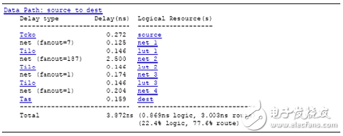
Figure 5-15 Schematic diagram of timing report with too high fanout
The corresponding solutions are:
1) Reduce the high fanout of the signal by means of logical copying, either manually in the HDL code or by setting it in the synthesis tool;
2) Area constraints can be used to put related logic together, although this method is limited to advanced users.
201-400Kva Diesel Generator,Super Silent Power Generator,400Kva Diesel Generator,Super Silent Type Diesel Generator
Shanghai Kosta Electric Co., Ltd. , https://www.generatorksd.com