After Apple released the iPhone X with Face ID, the discussion about 3D sensing has increased. Here, we are doing a super detailed professional science for this industry.
What is a 3D camera? The 3D camera is characterized in that in addition to being able to acquire a planar image, depth information of the subject, that is, three-dimensional position and size information, which is usually composed of a plurality of camera + depth sensors, can be obtained. The 3D camera realizes real-time 3D information collection, adds object sensing function to the consumer electronic terminal, and introduces multiple “painful application scenariosâ€, including human-computer interaction, face recognition, 3D modeling, AR, security and assisted driving. Multiple areas. Standing at the current time, we believe that the transition from 2D to 3D camera will be the fourth revolution after black and white to color, low resolution to high resolution, static image to motion picture, and it is expected to detonate the consumer electronics supply chain again! In a word, the touch screen implements the interaction from one dimension to the plane, while the 3D camera will change the interaction mode from plane to solid.
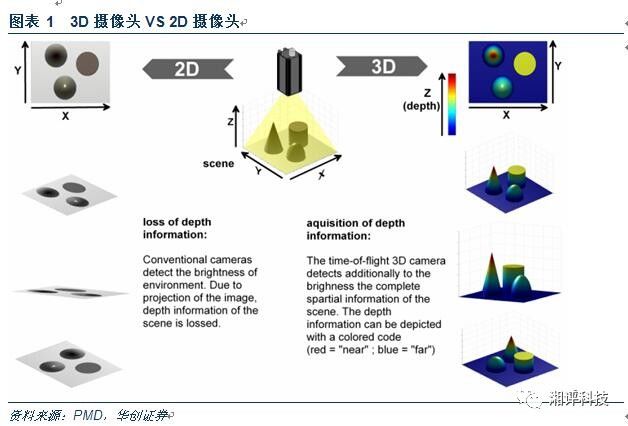
In terms of consumer experience, what kind of disruptive application can you achieve? The 3D camera acquires the depth information, three-dimensional size and spatial information of the environmental object in real time, and provides basic technical support for the “painful point†application scenarios such as motion capture, 3D modeling, VR/AR, indoor navigation and positioning, and thus has extensive consumption. Level and industrial application requirements. From the application point of view, the current scenes that 3D cameras can show their talents mainly include motion capture recognition in the field of consumer electronics, face recognition, 3D modeling in the field of automatic driving, cruising and obstacle avoidance, and parts scanning and sorting of industrial automation. Monitoring in the security field, statistics, and so on.

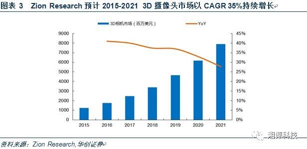
We believe that with the introduction of 3D camera technology by major customers this year, face recognition and gesture recognition applications will be the first to stand out, and the market space is expected to usher in explosive growth! According to research firm Zion Research, the 3D camera market will grow from $1.25 billion in 2015 to $7.89 billion in 2021, with an average annual growth rate of 35%! From the current industry chain research, the unit price is expected to be 13-18 US dollars; according to the 20% penetration rate of 1.8 billion smartphones in 2021, it has exceeded 10 billion US dollars in market space, plus in AR, autonomous driving, robotics and other fields. The entire 3D camera market space is expected to exceed $20 billion!
(B) "painful point type" application scenarios emerge one after another, will usher in the outbreak of mobile phone standard to smart terminal contention
1. Scene 1 - Face recognition comes in the first year, and fingerprint recognition stands out
Under the background of smart phones emphasizing differentiation and seeking innovation, face recognition is expected to become the next major innovation direction of consumer electronics and bring investment opportunities in the industry chain.
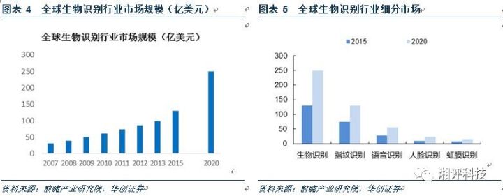
From the perspective of market share, the most likely to stand out after fingerprint recognition is face recognition. According to the China Foreground Industry Research Institute, the global market for biometrics grew at an average annual rate of 21.7% from 2007 to 2013. From 2015 to 2020, the market size of each segment is: fingerprint (73.3%), voice (100%), face (166.6%), iris (100%), and others (140%). Among the many biometric technologies, face recognition ranks first in terms of growth, and the market for face recognition technology is expected to rise to $2.4 billion by 2020. We expect the market size to be larger than expected in the case of smart terminals penetrating face recognition.
At present, the solutions of the face recognition market mainly include: 2D recognition, 3D recognition and thermal recognition. 2D face recognition is a method based on planar image recognition, but since the face of a person is not flat, 2D recognition has loss of feature information in the process of planarizing projection of 3D face information. 3D recognition uses a 3D face stereo modeling method to maximize the retention of valid information. Therefore, 3D face recognition technology is more reasonable and has higher precision.
The 3D camera technology represented by TOF and structured light is the most suitable for the face recognition technology. First of all, the 3D camera uses infrared light as the light to emit light, which can solve the problem of ambient light effects of visible light. When the traditional 2D recognition technology changes the ambient light, the recognition effect will drop sharply and cannot meet the needs of the actual system. For example, the "yin and yang face" phenomenon that occurs when you encounter a sidelight when taking a picture may not be recognized correctly.
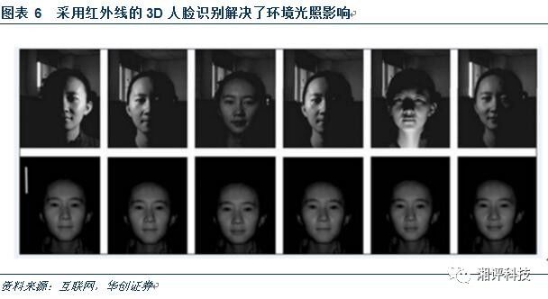
The TOF or structured light 3D camera technology captures the depth information of the face image when shooting, and can acquire more feature information to greatly improve the recognition accuracy based on the traditional face recognition technology. Compared with 2D face recognition system, 3D face recognition can collect depth feature information such as eye corner distance, nose point, nose point, distance between two temples, distance from ear to eye, and these parameters generally do not follow A person undergoes a large change in face-lifting and hair-dressing, so that 3D face recognition can continue to maintain a very high recognition accuracy when the user feature is issued.
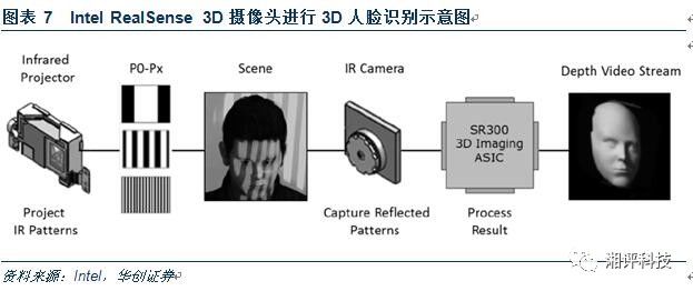
2, scene 2 - gesture recognition: the core pain points of human-computer interaction
Reviewing the development of human-computer interaction is actually a process of constantly transforming the machine to liberate people. In the earliest computers, the keyboard was the only input device. With the appearance of the GUI of the graphical interface, a combination of “keyboard and mouse†was formed. However, precise mouse clicks and keyboard typing still require high learning costs. After that, the smaller the device terminal is, the more the user is liberated, and the appearance of the touch screen of the mobile phone really gets rid of the intermediate medium of the mouse and the mouse, and achieves the hit-through. The next decade of human-computer interaction will be more intelligent and convenient, freeing users from touching the screen, actively capturing user gestures and performing recognition processing will become the next interactive pain point!
The key to gesture recognition lies in the 3D camera (or 3D perception) technology. The 3D camera uses TOF or structured light technology to obtain image depth information, and the user gesture is recognized by algorithm processing, thereby realizing the user to control the smart terminal. According to the MarketsandMarkets study, the market size of proximity sensors is expected to reach $3.7 billion in 2020 and a compound growth rate of 5.3% from 2015 to 2020.
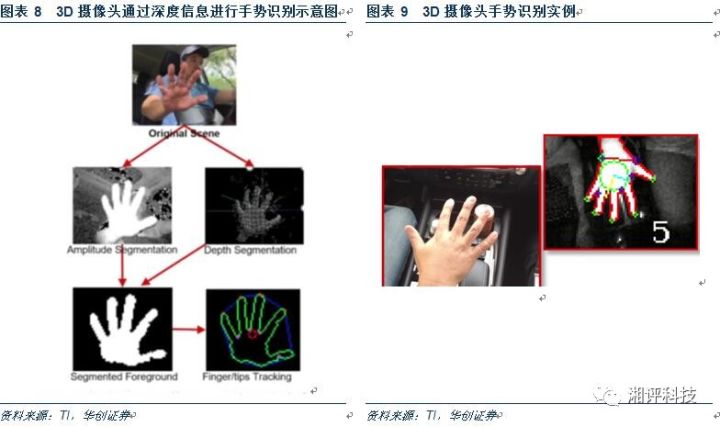
3, scene 3 - 3D reconstruction of the basic technology, AR / VR field will shine
Why should AR/VR equipment adopt 3D camera technology? ——1. Obtain RBG data and depth data of surrounding environment images for 3D reconstruction; 2. Implement human-computer interaction methods such as gesture recognition and motion capture.
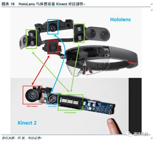
The 3D sensing of AR/VR generally adopts two active sensing technologies, TOF and structured light. The front of the device usually includes an infrared emitter, an infrared sensor (acquiring depth information) and multiple ambient light cameras. RBG information). Taking the TOF technology as an example, the infrared emitter emits infrared rays, and is reflected by the infrared sensor after being reflected by the target object, and the distance/depth data is obtained by calculating and converting the phase difference between the transmitted signal and the received signal.
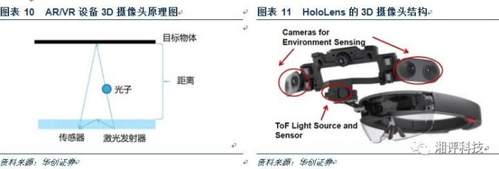
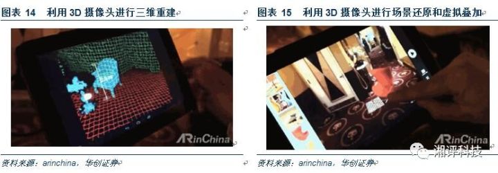
In the early stage, the three-dimensional model in the scene was reconstructed by two-dimensional images with different angles, and the realism was low. The appearance of the depth camera greatly improved the three-dimensional reconstruction effect. The depth camera can simultaneously acquire the RGB data and depth data of the image and perform 3D reconstruction based on this.
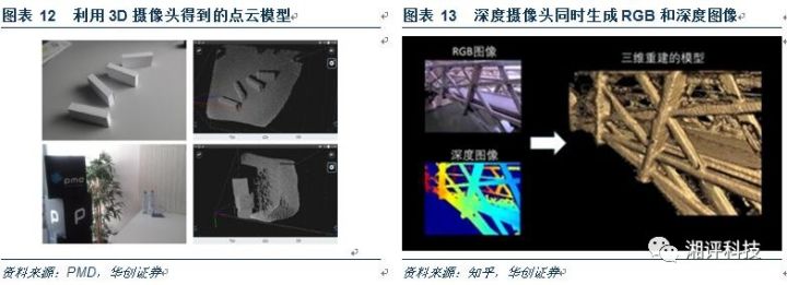
The following describes a three-dimensional reconstruction using a 3D camera through a simple scenario. A 3D camera based on TOF/structured light technology can be used to create a “point cloud†of the surrounding environment, as shown on the left, and different distances from the lens by different colors. The point cloud data combined with the RBG information of the environment image can be used to restore the scene as shown in the right figure, after which multiple applications such as ranging, virtual shopping, decoration, etc. can be derived, for example, the furniture placement in the right picture is performed. Since the restored scene has deep information, the simulated furniture cannot continue to push when it encounters obstacles, and it has super realism.
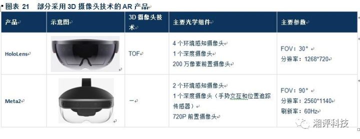
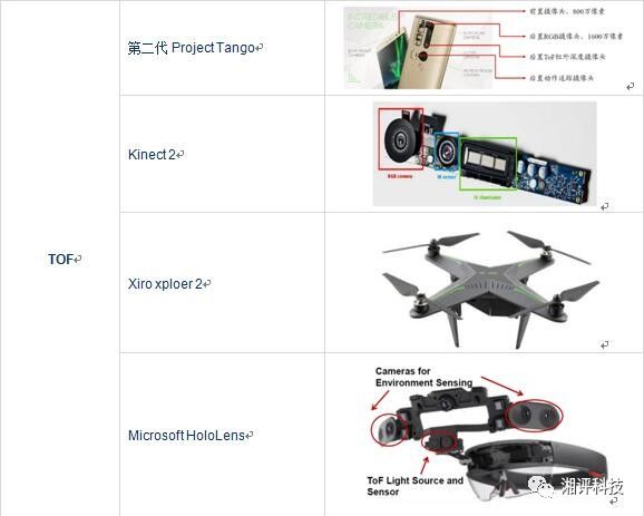
At the same time, the gesture recognition function provided by 3D camera technology will become the core interaction means in the future AR/VR field. At present, most VR devices introduced by major manufacturers require controllers. The advantage of game controllers is that control feedback is timely and combined. The disadvantage is that there is less interaction with the virtual environment, and the user can only control but not participate. In the AR application, the handle is completely incapable of the task of human-computer interaction. There is a wealth of human-computer interaction content in the AR application field, and this kind of interaction is very complicated, and only gesture operations can be completed. Taking HoloLens as an example, there is a set of four environment-aware cameras and a depth camera. The environment-aware camera is used for human brain tracking, and the depth camera is used to assist gesture recognition and perform three-dimensional reconstruction of the environment.

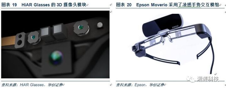
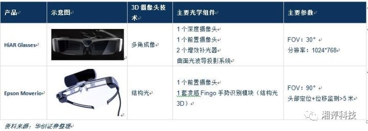
In addition to Hololens, AR products such as Meta2, HiAR Glasses and Epson Moverio have also adopted 3D sensing technology for gesture recognition and motion capture. We expect 3D cameras based on TOF or structured light technology to be used for gesture recognition and 3D. The basis of scene reconstruction will become the standard for AR equipment!
Second, 3D Sensing camera: a "premeditated" change iPhone8 introduction has been on the string!
(1) The technical route has matured: TOF and structural light
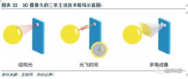
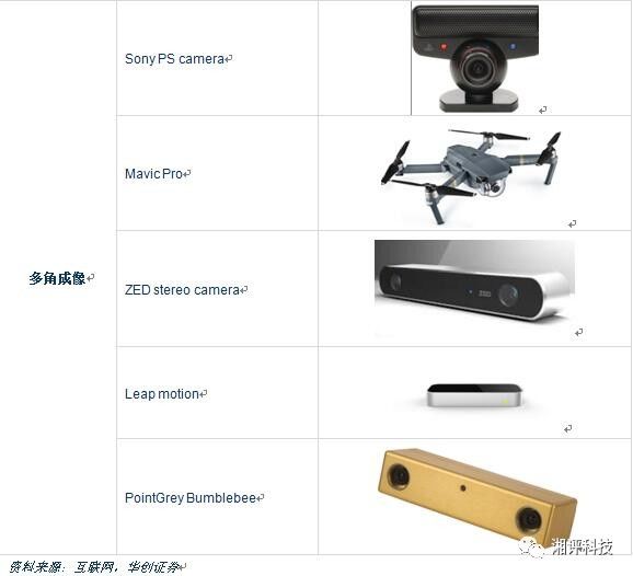
The 3D camera has three main technical routes: TOF (time of flight), structured light (structure light) and multi-angle imaging (also known as binocular stereo vision technology, multi-camera). From the current technological development and product application, TOF and structured light are the most promising due to their advantages of convenient use and low cost.
1. Time Of Flight technology
The TOF technology is to actively transmit the modulated continuous optical pulse signal to the target surface, and then use the sensor to receive the reflected light, and use the phase difference between them to calculate and convert the distance/depth data.
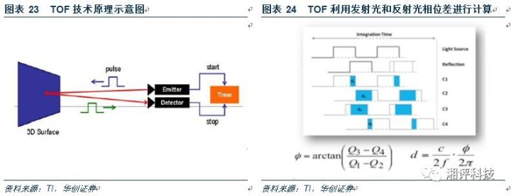
The advantage of TOF is that it can calculate the depth of pixel by pixel. The accuracy can be high in close range. The disadvantage is that the outdoor is affected by natural light and infrared rays, the measurement range is narrow (the distance cannot guarantee the progress), and the cost is more than the structural light. high.
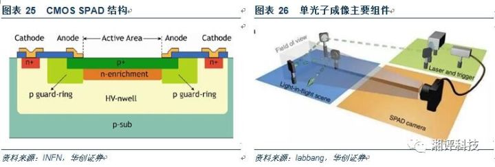
The current mainstream technology TOF technology uses a SPAD (single-photonavalanche diode) array to accurately detect and record the time and space information of photons, and then perform three-dimensional reconstruction of the scene through a three-dimensional reconstruction algorithm. SPAD is a kind of high sensitivity semiconductor photodetector, which is widely used in the field of low light signal detection.
2, structure light (structure light) technology
The basic principle of structured light technology is to place a grating outside the laser, and the laser will refract when it is projected through the grating, so that the laser will eventually shift at the falling point on the surface of the object. When the object is closer to the laser projector, the displacement caused by the refraction is smaller; when the object is farther away, the displacement caused by the refraction will correspondingly become larger. At this time, a camera is used to detect and collect the pattern projected onto the surface of the object. Through the displacement change of the pattern, the position and depth information of the object can be calculated by an algorithm, thereby restoring the entire three-dimensional space.
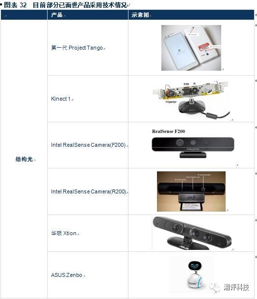
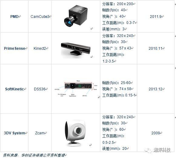
Representative products using structured light technology include Kinect 1, Intel RealSense Camera (F200 & R200) ​​and first-generation project tango products.
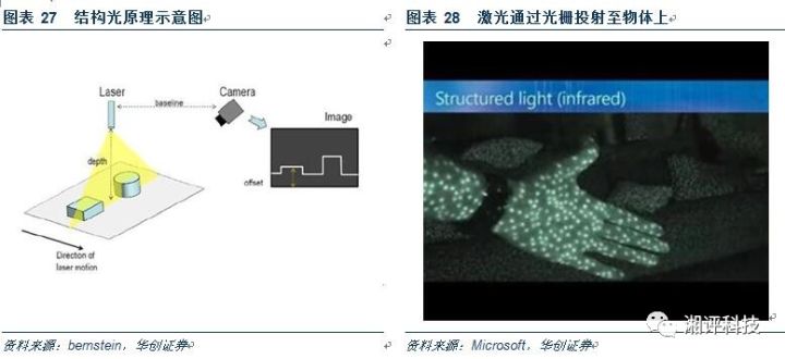
The advantage of structured light technology is that the depth information can be read in one imaging. The disadvantage is that the resolution is limited by the grating width and the wavelength of the light source, and the requirements for the diffractive optical device (DOE) are also high, and the infrared light of the visible light is also greatly affected.
3. Multi-Camera technology
Multi-angle imaging technology is based on the parallax principle, and uses the imaging device to acquire two images of the measured object from different positions, and obtains the three-dimensional geometric information of the object by calculating the positional deviation between the corresponding points of the image.

The advantages of the multi-angle imaging technology are that both indoor and outdoor applications are not affected by sunlight and are hardly affected by the transparent barrier. The disadvantage is that the calculation amount is large, the algorithm is complicated, and the hardware has high requirements.
The following table compares three mainstream technologies from software complexity, latency, active illumination, detection distance, resolution, and more:
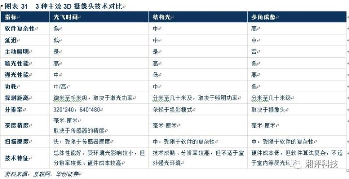
Judging from the application of the products already on the market, the application of structured light/TOF is mature, and the technical principle is the same. Most of the original products use structured light technology, and the number of TOF technologies in the new generation is gradually increasing. We believe that TOF technology will become the most promising future in terms of its advantages in software complexity, delay, precision, and scanning speed. 3D camera technology; while structured light has a good advantage in cost advantages, one-time imaging, etc., is expected to become the vanguard of mobile applications.
(2) The international consumer electronics manufacturers have mature 3D Sensing camera technology. Apple's accumulation is the deepest.
Since 2009, major consumer electronics giants have begun to deploy 3D camera fields, and there have been signs of acceleration in the past two years! In recent years, giants represented by Intel, Microsoft, Sony and Qualcomm have launched mergers and acquisitions in the fields of TOF 3D sensors, gesture recognition algorithms, and downstream application software solutions.
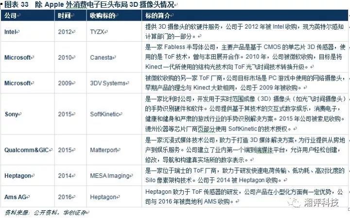
Apple has been in the 3D camera technology and its downstream applications for a long time, we expect the iPhone 10th anniversary model is expected to sacrifice this killer technology. Throughout the history of consumer electronics innovation, large end customers have the ability to cultivate emerging markets, lead innovation trends, and drive technological innovation in the industry. Once high-end manufacturers of other manufacturers are required to follow up quickly, the entire industry is expected to usher in explosive growth.
Apple first deployed in the 3D camera field in 2010, and has acquired a number of 3D imaging, face recognition and gesture recognition companies. In September 2010, the acquisition of Swedish algorithm company Polar Rose, the acquisition of Prime Sense in 2013, the acquisition of machine learning and image recognition company Perceptio in 2015 and the Israeli 3D camera technology company LinX, and the motion capture company Faceshift, Apple in 2016 Acquisition of face recognition system company Emotient.
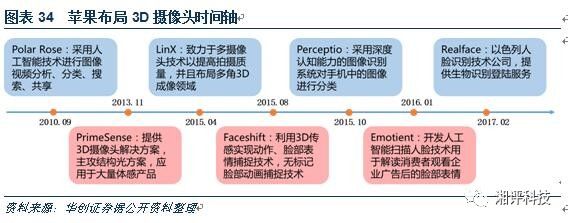
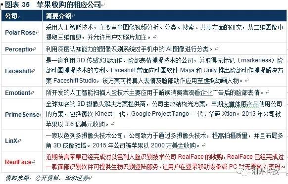
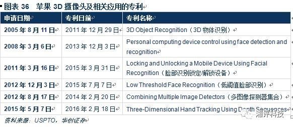
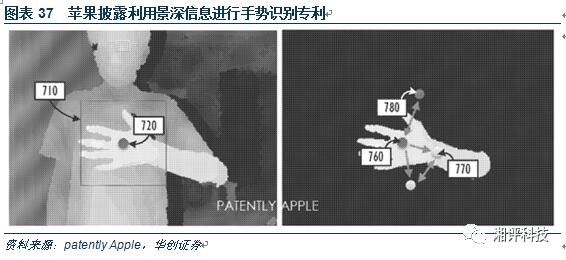
In terms of patents, Apple began patenting 3D camera technology and related applications since 2005, including gesture recognition using image depth information and face recognition using devices such as infrared sensors.
(3) The application of the iPhone in the distance sensor has been in full swing. The 3D Sensing camera is deployed in the tenth anniversary edition.
Compared with 3D Sensing's distance sensor application, which is similar in basic structure and basic principle, Apple has become a standard since the iPhone 3GS. Below we comb the innovations of the iPhone's pre-structure from the structure, principle and function.
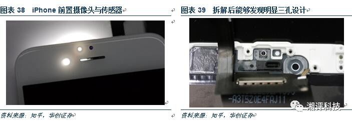
Apple has a front-end distance sensor design from the original iPhone. It is mainly used to judge the distance between the user's head and the screen. When the phone is close to the ear, it can automatically close the screen. All previous iPhones have two front sensors (ambient light sensor + infrared distance sensor) and a front camera: from right to left are front camera, light sensor, infrared distance sensor, where the optical sensor is usually covered by ink and cannot be found.
Distance sensor: use an infrared diode to emit infrared light. If there is an object close to it, it will reflect infrared light. The reflected infrared light is perceived by the infrared light detector, and the signal is transmitted to the CPU through some column logic control operations. The CPU can control whether the screen wakes up or not.
Ambient light sensor: It is mainly used to detect changes in optical signals in the environment and then convert their changes into digital signals for output to the CPU.
Theoretically, the distance sensor consists of two units, transmitting and receiving, but why is there only three holes in the front? This is because Apple adopts a method of integrating the ambient light sensor and the distance sensor receiving end. Two photodiodes are used in the distance sensor: one broadband photodiode detects the optical in the 300nm~1100nm band, and the other uses the narrowband filter material. The infrared light is detected, and then the infrared light is subtracted from the light received by the broadband photodiode to obtain an ambient light signal.
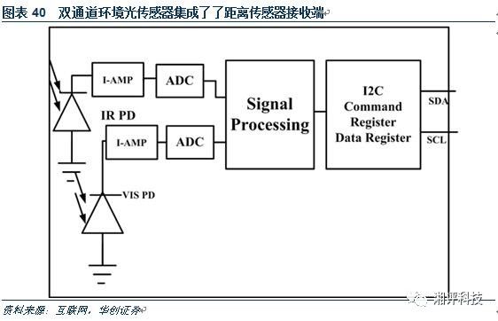
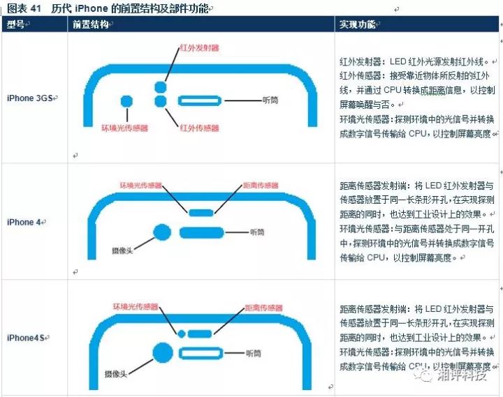
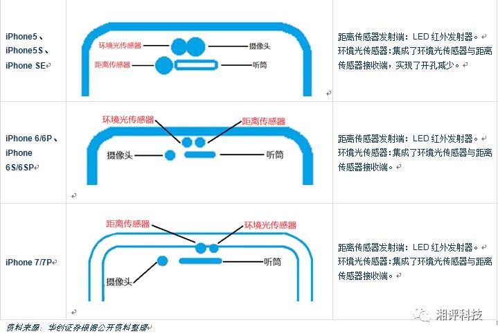
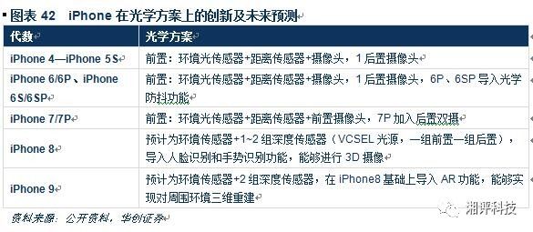
It can be seen that the front-end structure of the iPhone includes a front camera, a distance sensor and an ambient light sensor. The only innovation is whether to integrate the distance sensor receiving end with the ambient light sensor, and the function can only realize whether the user's head is close to the function. The handset controls the screen. We believe that the application of the distance sensor for 8 consecutive generations shows that Apple has designed and used the ranging module on the mobile phone.
We conclude that the introduction of a 10D camera technology based on structured light or TOF technology for a large customer's 10th anniversary model will be a high probability event, and the 3D camera module is likely to be more than one! This technology will bring 3D face recognition and gesture recognition to a new generation of products, opening a new wave of consumer electronics innovation trends!
Third, decrypt the 3D Sensing camera industry chain The biggest change lies in the IR VCSEL module (light source + optical components)
(1) Dismantling the 3D Sensing camera
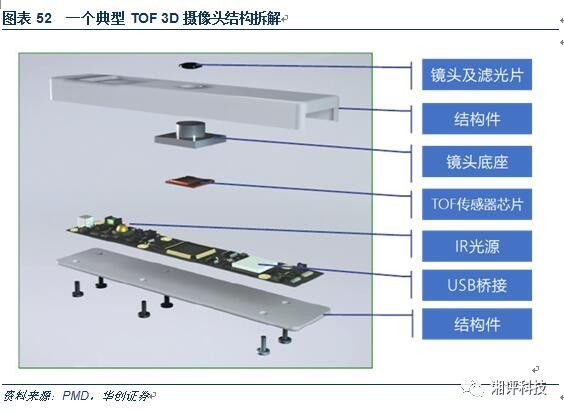
3D camera introduces 3D sensing technology based on TOF or structured light on the basis of traditional camera. At present, these two mainstream 3D sensing technologies are active sensing. Therefore, the 3D camera industry chain mainly adds infrared light source + optical compared with the traditional camera industry chain. Components + infrared sensors and other parts.
The following is a breakdown of the 3D camera industry chain with specific product disassembly. First, take the Lenovo Phab 2 Pro phone on the Google tango platform as an example. Tango is an augmented reality computing platform developed and authored by Google. It uses computer vision to enable mobile devices, such as smartphones and tablets, to detect their location relative to the world around them without the need for GPS or other external signals.
The back structure of the Lenovo Phab 2 Pro mobile phone on the Tango platform, from top to bottom, is the main camera, infrared sensor, infrared emitter, flash, motion tracking camera, fingerprint recognition module.
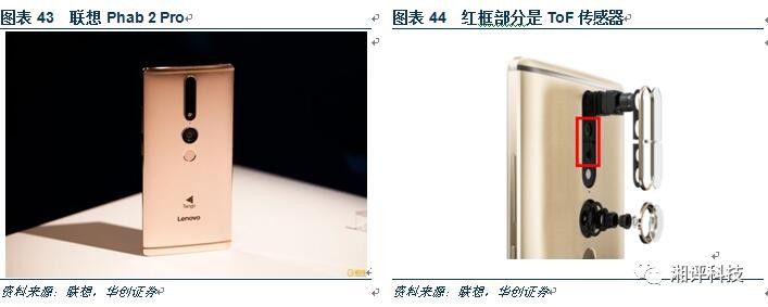
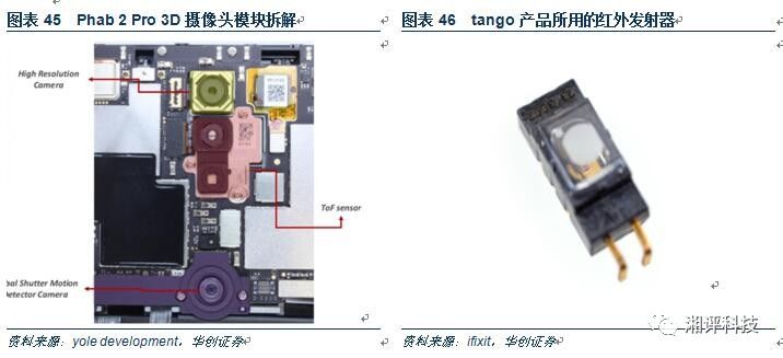
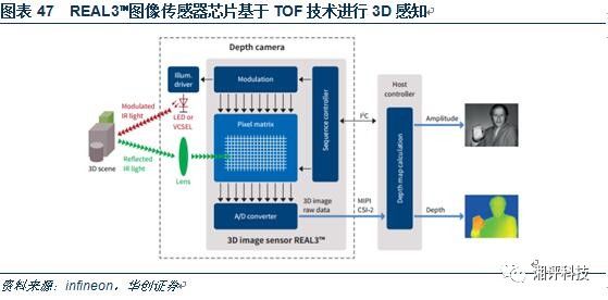
The Phab 2 Pro's 3D camera module uses the REAL3TM image sensor chip developed by Infineon and PMD tec. This chip combines analog and digital signal processing with high data rates. It integrates a pixel array, control circuitry, ADC, and digital high-speed interface on a single chip.
Let's take the example of RealSense 3D camera developed by Intel. This 3D camera product is based on structured light technology and is also an active sensing technology.

The RealSense 3D camera is mainly composed of an infrared camera, a normal camera, an infrared laser transmitter and a dedicated chip (SR300 ASIC): the laser emitter emits infrared light and is irradiated onto the surface of the object via a grating, and the camera detects the collection and projection onto the surface of the object. The pattern can be used to calculate the position and depth information of the object by the displacement of the pattern.
By disassembling and analyzing the mainstream 3D camera products already on the market, the 3D camera industry chain can be divided into:
1. Upstream: infrared sensor, infrared light source, optical component, optical lens and CMOS image sensor;
2. Midstream: sensor module, camera module, light source foundry, light source detection and image algorithm;
3. Downstream: terminal manufacturers and applications.
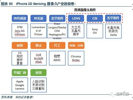
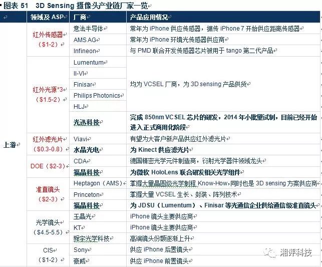
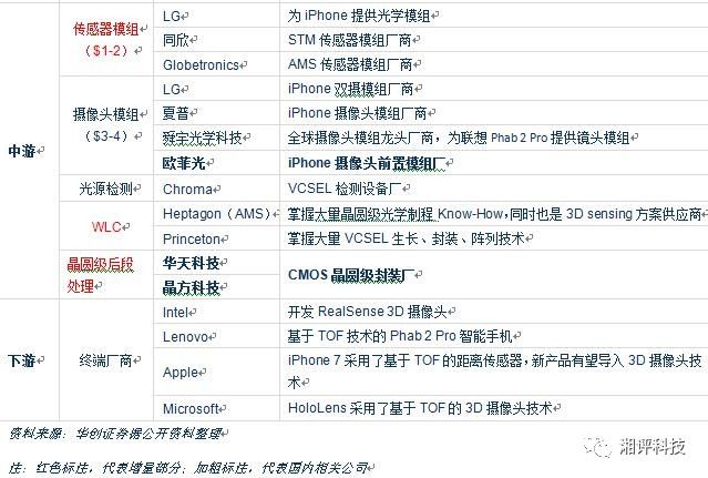
The key components of the 3D camera industry chain are: 1. Infrared sensor; 2. Infrared laser source; 3. Optical components.
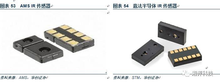
(2) One of the key points - Infrared sensor: a high version of the distance sensor No domestic enterprise can cut in
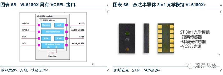
The high version of the distance sensor, although critical, is not purely elastic. Infrared sensors are currently divided into AMS (Austrian Microelectronics) / Heptagon and STMicroelectronics. TI and infineon also have layouts in this field. AMS has supplied ambient light sensors for Apple since the iPhone 4, and its Heptagon has been working on miniaturization of TOF sensors and was acquired by AMS in 2016. In recent years, STMicroelectronics has developed several 3D camera modules that integrate infrared sensors and infrared laser emitters. The VL6180X solution based on TOF technology has been adopted by the iPhone 7 as a distance sensor. Infineon has partnered with TOF Fabless PMD to develop the REAL3 3D image sensor chip, which has been used in tango's second generation. At present, the gap in the sensor field in China is relatively obvious. In the short term, there will be no breakthroughs for related companies; from the perspective of investment, we will not focus on analysis.
(3) The second key point - IR VCSEL: from optical communication to consumer electronics
As we mentioned before, the application of lasers will be a big direction and trend in the future; there are many types of laser processing components with complex and matching lasers. We will take the lead in the market to conduct an exclusive analysis, and strive to find the most likely target and lay the foundation for follow-up research. We boldly predict that after the future of laser consumer applications, the upgrade and adjustment of laser technology will accelerate, just as the touch screen is launched, GG/GFF/GF/OGS/In Cell/On Cell and other technologies are coming. . Here we take the lead..
This section focuses on the following five issues:
1) What is VCSEL?
2) Why use VCSEL as a light source for consumer electronics applications?
3) What mainstream players are there in the VCSEL industry?
4) From the perspective of overseas mapping, how does VCSEL expand from the field of optical communication to the field of consumer electronics?
5) What is the future development trend of VCSEL? Consumer electronics applications will create conditions for further expansion of VCSEL
1. What is VCSEL?
A VCSEL (Vertical-Cavity Surface-Emitting Laser) is a semiconductor laser that emits laser light perpendicular to the substrate surface. The basic structure is a "sandwich" structure consisting of three upper and lower DBR mirrors and an active area. The upper and lower DBR mirrors and the active area form a resonant cavity. The active region consists of several quantum wells. As the core part of the VCSEL, it determines the important parameters such as the threshold gain and lasing wavelength of the device. The high reflectivity DBR consists of a multilayer dielectric film set that provides feedback to light. In order to obtain a smaller threshold current, the reflectivity of the DBR mirror is generally above 99.5%.
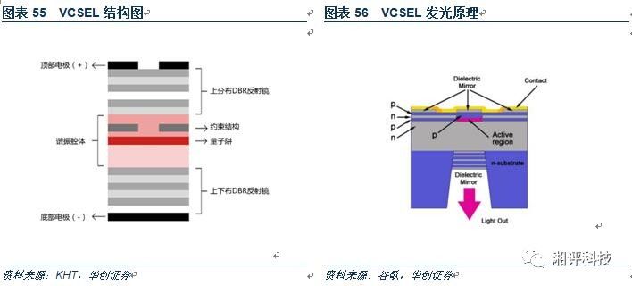
Commonly used raw materials for VCSELs are luminescent compound semiconductors such as gallium arsenide, indium phosphide or gallium nitride. In terms of the principle of luminescence, VCSEL is the same as other semiconductor laser illuminating principles. The first thing to achieve is energy excitation. The electrons that excite the semiconductor by the applied energy are transitioned from the valence band to the conduction band. When the electron is returned from the conduction band to the valence band, the energy is converted into light energy. The type is released. Then, relying on the upper and lower DBR mirrors and the resonant cavity composed of the gain material to achieve resonance amplification, the resonant cavity causes the excited light to be reflected between the upper and lower DBR mirrors, and continuously absorbs light energy through the light-emitting region, so that the laser is received. A plurality of energy feedbacks form a laser.
2. What should I use VCSEL as the light source for consumer electronics applications?
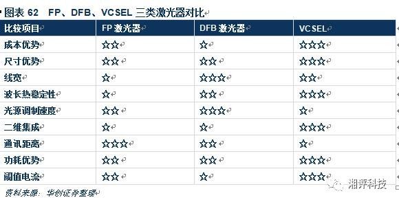
The reason is that VCSEL combines the advantages of low manufacturing cost, excellent performance and easy integration! After years of development in the fields of telecommunications, data communication, etc., VCSEL has the characteristics of high coupling efficiency, low power consumption, fast transmission rate and low manufacturing cost. Compared with LED and FP lasers and DFB lasers, it has the advantages of small volume, circular output spot, single longitudinal mode output, small threshold current, low price, easy integration into large-area arrays, etc., widely used in optical communication and optical interconnection. , optical storage and other fields.
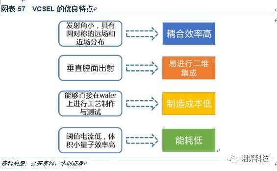
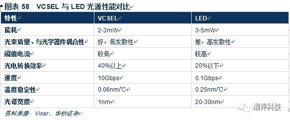
Why use VCSEL without LED? Actively aware 3D camera technology typically uses infrared light to detect targets, and early 3D sensing systems typically use LEDs as infrared sources. In terms of technology, since the LED does not have a resonator, the beam is more divergent and is not as good as VCSEL in terms of coupling. Because VCSELs are superior in terms of accuracy, miniaturization, low power consumption, and reliability, common 3D camera systems generally use VCSELs as infrared sources.
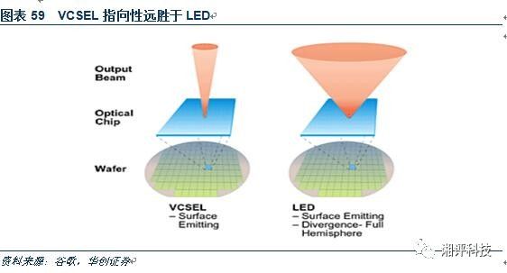
Semiconductor lasers can be divided into edge-emitting lasers and surface-emitting lasers according to the direction of emission. Among them, edge-emitting lasers mainly include FP lasers and distributed feedback lasers (DFB lasers). Refers to VCSEL.
The FP laser is generally composed of a substrate layer, a waveguide layer, an active layer, and a metal wire layer. A double heterojunction multi-quantum well active layer is generally used; the DFB laser is added along the FP to the outside of the common cavity. The layer grating relies on the frequency selection principle of the grating to realize the longitudinal mode selection to enhance the monochromaticity of the laser; the sandwich structure of the VCSEL has been introduced before.
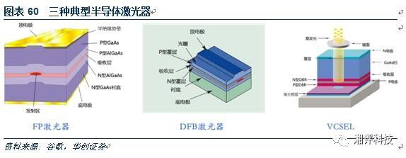
Compared with conventional edge-emitting lasers, VCSELs have great advantages in beam quality, fiber coupling efficiency, and cavity surface reflectivity, and because VCSEL emits light perpendicular to the substrate while the emitting laser emits light parallel to the substrate, VCSELs are capable of implementing two-dimensional arrays while emitting lasers. ,
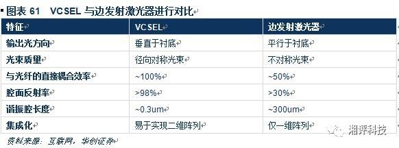
We compare and analyze three mainstream semiconductor lasers in terms of cost advantages, size advantages, wavelength thermal stability, power consumption, and communication distance:
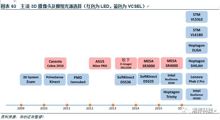
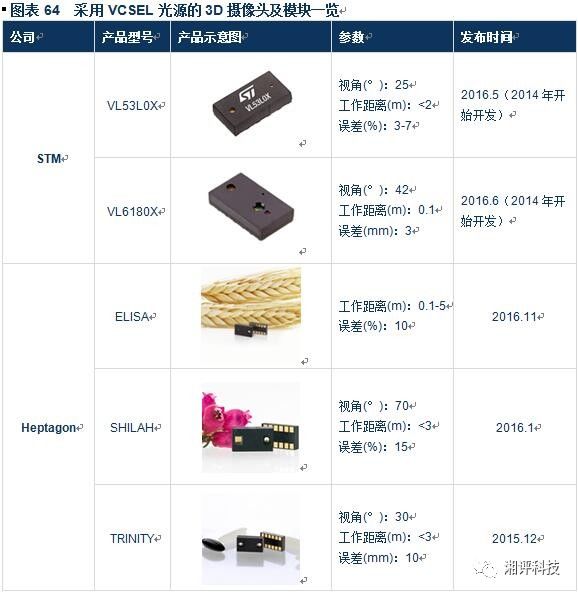
It can also be seen from the recently launched products with 3D cameras that the conversion of infrared light sources from LEDs to VCSELs is a certain trend! From the new optical module products released by STMicroelectronics and AMS's Heptagon in 2016, VCSEL is used as the infrared light source, and the consumer-grade Lenovo Phab 2 Pro AR mobile phone and Intel RealSense SR300 also use VCSEL as the infrared light source.
3. What are the big players in the VCSEL field?
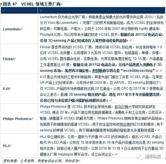
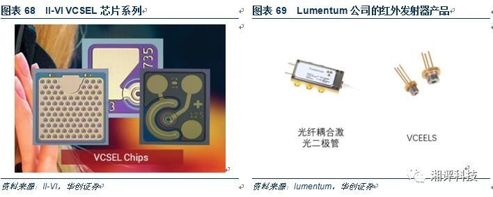
At present, there are five major manufacturers in the VCSEL field, namely Lumentum, Finisar, II-VI, Philips Photonics and HLJ Hualijie. We can see that basically all of them are leading companies from optical communication chips; it can be said that it is the experience of optoelectronics in the field of communication, consumer-grade applications have become logical, and both products have strong technical scalability. Focus on the optoelectronic communication leader and cut into the explosive potential of consumer electronics applications.
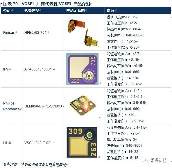
4. From the perspective of overseas mapping, how does VCSEL expand from the field of optical communication to the field of consumer electronics?
We analyzed the development history of VCSEL devices in combination with the product line changes of industry leaders Finisar and Lumentum.
1) One of the overseas maps: Lumentum of VCSEL big players
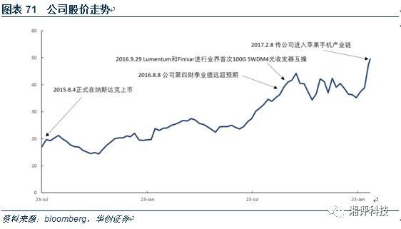
Lumentum is the industry's leading supplier of optical products. Its predecessor was JDSU, the absolute leader in optical communications (JDSU split in 2015, the independent CCOP business unit was named Lumentum, and the NE, SE and OSP business units were renamed Viavi). The company currently offers solutions based on optical optoelectronics for applications such as data communications, telecommunications networks, commercial lasers and 3D sensing in consumer electronics.
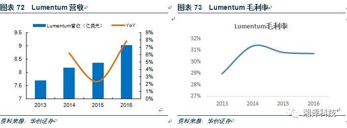
Due to the large number of data centers established in recent years and the strong demand for 100G data communication products, the company's revenue has maintained steady growth, with revenue of 903 million US dollars in FY2016. Benefiting from the development of high-end optical components, optical modules and commercial laser products, the company's gross profit margin is on the rise, and the gross profit margin has remained above 30% in the past three years.
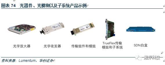
At present, the company's products are mainly divided into optical communication optical devices and optical modules, industrial laser diodes and 3D Sensing three areas. Relying on the deep advantages of optical devices and optical modules, the company has developed "vertical + horizontal" in recent years:
Vertically, the company has developed vertically, achieving vertical integration production from wafer design and manufacturing, optical device sub-components, and optical module integration;
Horizontally, the company is actively expanding its product lines and applications outside the field of optical communications. With its strong vertical integration capability, it is able to apply industrial-grade applications such as industrial inspection and measurement, commercial-grade applications such as medical imaging and consumer electronics 3D sensing technology. Expanded, currently achieving comprehensive coverage of various types of optical device applications.
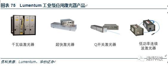
In the industrial application of laser product line, the company's main products are kilowatt lasers, ultrafast lasers, Q-switched lasers and low-power continuous wave lasers. At present, mainstream applications are divided into machining of large devices and machining of micro-miniature devices. The machining of large-scale devices is mainly applied to the processing of large materials such as automobiles and aerospace, while the machining of micro-miniature devices is mainly applied to the processing of small materials such as mobile phone screens and medical devices.
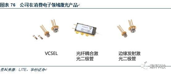
The company's laser line in the consumer sector includes VCSELs, edge-emitting laser diodes and fiber-coupled laser diodes. Among them, VCSEL is the company's absolute ace in this field, which can be mainly applied to gesture recognition of smart terminals, eye tracking of mobile devices, face recognition and so on.
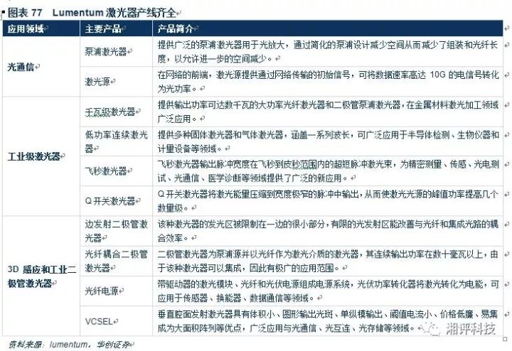
At present, the company mainly faces the four major markets of telecommunications, data communication, industrial laser and 3D Sensing. The largest proportion of revenue is in the telecommunications market, accounting for 62%; followed by the data communications market, accounting for about 18%; industrial lasers accounting for about 19%; 3D Sensing business accounting for about 1%.
Benefiting from the company's continued advantages in the telecommunications and data communications markets, optical communications business increased by 8% quarter-on-quarter in the 2017Q2 quarter, up 27% year-on-year. Among them, the telecommunications network business revenue was US$160 million, an increase of 16.10% year-on-year and 3.3% quarter-on-quarter. The data center business performed strongly with revenue of US$60.1 million, an increase of 94.57% year-on-year and a growth of 54.1% quarter-on-quarter.
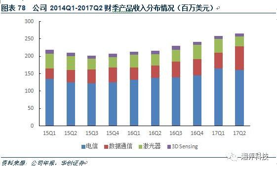
Although the current 3D Sensing products account for a relatively low total revenue of the company, from the company's annual report disclosure, the company's significantly increased R&D expenses in the 2016~2017 fiscal year are mainly directed to the 3D Sensing business. Combined with the current industry chain research and 2014 history, the company's 3D sensing business is expected to start explosive growth in 2017~2018!
Here we make a simple calculation. In 2014, about 20 million Kinect II products were shipped using the company's 3D sensing products, which brought nearly $50 million in revenue to the company. We assume that the high-end models with 3D cameras in 2017 will reach 50 million, and one mobile phone will be equipped with two VCSEL components. The company will supply VCSEL devices with ASP for $1.5 and the company with 70% share, which is expected to bring 105 million to the company. The dollar performance has increased!
2) Overseas mapping 2: Finisar of VCSEL big players
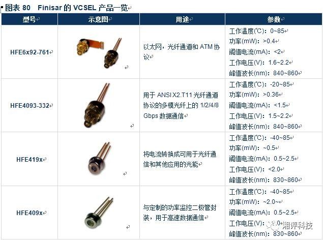
Finisar is the world's leading VCSEL manufacturer and continues to lead VCSEL applications. In recent years, VCSEL shipments have remained at more than 150 million units. At present, the company's VCSEL device products are close to 30 kinds, and the company's products are highly flexible and scalable, allowing customers to customize VCSEL arrays to meet various application requirements.
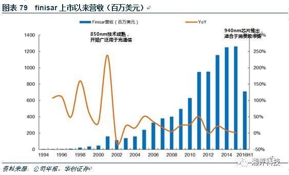
Finisar's products were originally used in the field of optical communications such as telecom, datacom, etc., mainly used in radio transceivers TxRx, active optical cable AOC and embedded optical modules.
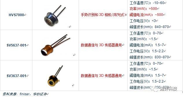
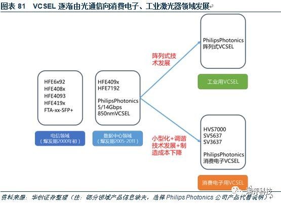
Since 2010, under the dual role of “external cause†+ “internal causeâ€, the company has gradually begun to deploy applications in the field of consumer electronics. "External causes" include the emergence of 3D camera technology and the miniaturization and low cost of VCSEL. The "internal cause" is that the company faces the homogenization competition by continuously introducing differentiated products through continuous research and development in the increasingly fierce market competition. The right to speak in pricing.
5, VCSEL development trend: high speed, high efficiency, low power consumption, low cost, consumer electronics applications will create conditions for further expansion
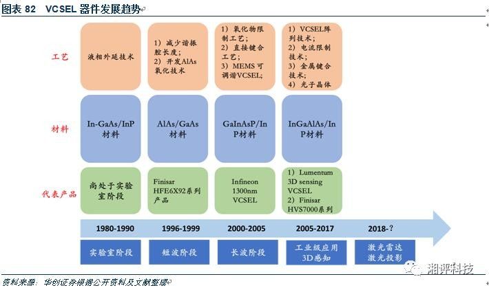
VCSEL器件由问世,到è¿ç”¨äºŽå…‰é€šä¿¡é¢†åŸŸï¼Œå†åˆ°å»¶ä¼¸è‡³æ¶ˆè´¹ç”µå领域,本质上是其性能ã€å·¥è‰ºå’Œæ料的一部å‘展å²ï¼Œä»ŽæŠ€æœ¯çœ‹äº§ä¸šï¼Œæˆ‘们结åˆVCSEL领域内主è¦çŽ©å®¶äº§å“线å˜åŒ–å’ŒVCSELå‘展历程探æžã€‚
1ã€1990-1996:该阶段VCSEL刚刚问世,主è¦æ˜¯é‡‡ç”¨æ¶²ç›¸å¤–延技术(LPE)实现In-GaAs/InPæ料。这时它在å„æ–¹é¢æ€§èƒ½å¹¶ä¸å…·æœ‰ä¼˜è¶Šæ€§ï¼Œå‘å°„æ–¹å¼ä¸ºè„‰å†²æ¿€å°„,ä¸å¿ƒæ³¢é•¿ä¸º1.18um,阈值电æµä¸º900mA(远大与æˆç†ŸæŠ€æœ¯ï¼‰ï¼›
2ã€1996-1999:该阶段主è¦æ˜¯650~850nmçŸæ³¢æ®µçš„大范围应用å‘展。业界主è¦é‡‡ç”¨å‡å°‘è°æŒ¯è…”长度的方法æ¥é™ä½Žé˜ˆå€¼ç”µæµï¼Œå¹¶é€šè¿‡å¼€å‘AlAs氧化技术æ¥æå‡DBRå射镜的å射率,具有高å射率ã€é«˜çƒä¼ 导率和良好的导电特性的AlAs/GaAs在这一阶段被应用于VCSEL,实现在850nm下超过80%çš„å射率,åŒæ—¶é˜ˆå€¼ç”µæµé™ä½Žè‡³mA级别。1997å¹´èµ·VCSEL在å•é€šé“çŸè·ç¦»å…‰å¦äº’连市场å æ®äº†ç»å¯¹çš„主导地ä½ï¼Œæ¤å¤–也在650~670nm波段被应用于基于塑料光纤的数æ®é€šä¿¡ç³»ç»Ÿï¼ˆå› 为塑料光纤在650nm处有最å°å¸æ”¶ï¼‰ï¼›
3ã€2000-2005:这一阶段主è¦æ˜¯1300nm\1500nm长波段的应用å‘展,主è¦è§£å†³æ³¢é•¿å˜é•¿å¸¦æ¥çš„æ•£çƒã€ç”µæµé™åˆ¶ã€å射镜制作ç‰é—®é¢˜ã€‚首先氧化物é™åˆ¶å·¥è‰ºè¢«å¼•å…¥ï¼Œè¿™ä¸€æŠ€æœ¯èƒ½å¤Ÿæžå¤§åœ°æå‡å…‰ç”µè½¬æ¢æ•ˆçŽ‡ï¼ˆ50%以上)和光æŸç¨³å®šåº¦ï¼Œä½¿å…¶èƒ½å¤Ÿç¨³å®šåœ°è€¦åˆè¿›å•æ¨¡å’Œå¤šæ¨¡å…‰çº¤ï¼ŒåŒæ—¶æ°§åŒ–物é™åˆ¶æ–¹æ¡ˆèƒ½å¤Ÿç»§ç»é™ä½Žé˜ˆå€¼ç”µæµè‡³å‡ 百μA,为解决æ¤åŽVCSEL阵列严é‡è¿‡çƒé—®é¢˜æ‰“下基础。åŒæ—¶ç›´æŽ¥é”®åˆå·¥è‰ºåœ¨é•¿æ³¢æ®µVCSEL制作ä¸å¾—åˆ°å¹¿æ³›åº”ç”¨ï¼Œå› ä¸ºé•¿æ³¢é•¿ææ–™GaInAsP/InP与DBR两ç§æ料折射率相差å°ï¼Œåå°„æ€§èƒ½å·®ï¼Œå› æ¤ç›´æŽ¥é”®åˆGaAs基DBR与InP有æºåŒºæ¥åˆ¶ä½œé•¿æ³¢æ®µVCSELæˆä¸ºçƒç‚¹ï¼Œé•¿æ³¢æ®µVCSEL是大容é‡å…‰é€šä¿¡ç³»ç»Ÿå’Œå…‰äº’连的关键器件;
4ã€2005-2016:这一阶段VCSEL器件开始é€æ¸ç”±å…‰é€šä¿¡é¢†åŸŸå»¶ä¼¸è‡³å·¥ä¸šçº§åº”用åŠæ¶ˆè´¹ç”µå领域,å‘展趋势为阵列化和å°åž‹åŒ–ã€‚è¿™ä¸€é˜¶æ®µæ ¸å¿ƒå·¥è‰ºä¸»è¦ä¸ºåŸºäºŽMEMS技术的å¯è°ƒè°VCSEL技术ã€VCSEL阵列技术以åŠç”µæµé™åˆ¶æŠ€æœ¯ã€‚阵列技术使得VCSEL器件å‘高功率ã€é«˜é€ŸçŽ‡å‘å±•ï¼Œå¾—ä»¥ç”¨äºŽåŠ çƒã€æŽ¢æµ‹ç‰å·¥ä¸šçº§åº”用领域。电æµé™åˆ¶æŠ€æœ¯ï¼ˆç¦»å注入ã€æŽ©åŸ‹éš§é“结ç‰ï¼‰å°†ç”µæµé™åˆ¶åœ¨è¾ƒå°åŒºåŸŸå†…,是VCSEL微型化的关键工艺。æ¤å¤–金属键åˆæŠ€æœ¯çš„引入改善了VCSELçš„æ•£çƒé—®é¢˜ï¼Œä½¿å¾—它能够更好地应用于体感设备ã€æ™ºèƒ½æ‰‹æœºç‰æ¶ˆè´¹ç”µå领域。
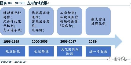
应用领域方é¢ï¼ŒVCSEL主è¦ç”±å…‰é€šä¿¡é¢†åŸŸåº”用å‘å•†ä¸šçº§åº”ç”¨å¦‚å·¥ä¸šåŠ çƒã€çŽ¯å¢ƒç›‘测ã€åŒ»ç–—以åŠæ¶ˆè´¹ç”µå应用如3D sensingå‘展。850nm波段VCSEL商用化程度最为æˆç†Ÿï¼Œæ˜¯çŸè·ç¦»å…‰çº¤æ•°æ®ä¼ 输系统的é‡è¦å™¨ä»¶ï¼›æ¤åŽå¼€å‘出的长波段产å“主è¦ç”¨äºŽé•¿è·ç¦»å…‰çº¤é€šä¿¡ã€å…‰å¹¶è¡Œå¤„ç†ä»¥åŠå…‰è¯†åˆ«ç³»ç»Ÿï¼›æ¤åŽéšç€å·¥è‰ºã€æ料技术改进,VCSEL器件在功耗ã€åˆ¶é€ æˆæœ¬ã€é›†æˆã€æ•£çƒç‰é¢†åŸŸçš„优势开始显现,é€æ¸åº”ç”¨äºŽå·¥ä¸šåŠ çƒã€çŽ¯å¢ƒç›‘测ã€åŒ»ç–—设备ç‰å•†ä¸šçº§åº”用以åŠ3D感知ç‰æ¶ˆè´¹çº§åº”用。
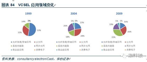
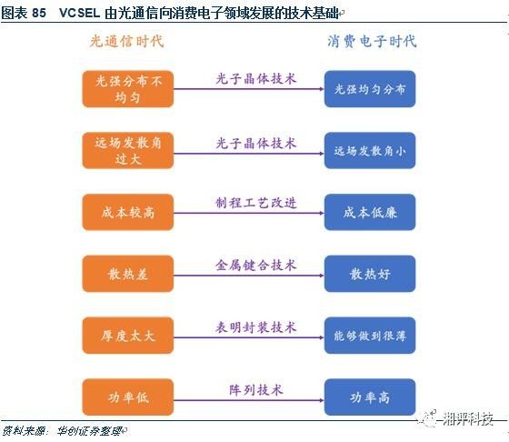
éšç€æŠ€æœ¯å‘展VCSEL在集æˆæ–¹é¢çš„优势也开始显现:1)å 用é¢ç§¯å°.一个器件大å°ä¸ºå‡ åˆ°å‡ åμm,与æ¡å½¢æ¿€å…‰å™¨çš„300μm相比更å°ï¼›2)从周围的å„个方å‘都å¯ä»¥å˜å–,而æ¡å½¢æ¿€å…‰å™¨åªé™äºŽä¸¤ä¾§ï¼Œä¸”其大å°å—è°æŒ¯è…”的长度é™åˆ¶ï¼›3)能够实现表é¢å°è£…(与边缘å‘射器的TO-canå°è£…相比大大å‡å°‘厚度);4)å¯æž„æˆäºŒç»´é˜µåˆ—。集æˆæ–¹é¢çš„优势使得VCSEL器件既å¯ä»¥é€šè¿‡æ¨¡å—化组装æˆä¸ºé«˜åŠŸçŽ‡é˜µåˆ—ä½œä¸ºåŠ çƒæ¿€å…‰å…‰æºä½¿ç”¨ï¼Œåˆèƒ½å¤Ÿå‡å€Ÿå°åž‹åŒ–优势应用于å„类消费电å产å“。
åˆ¶é€ å·¥è‰ºæ¥çœ‹ï¼Œä¸€ä¸ªå®Œæ•´çš„VCSEL从æ料到器件è¦ç»è¿‡æ料生长ã€å¤–延结构表å¾ã€å™¨ä»¶åˆ¶ä½œã€æ€§èƒ½æµ‹è¯•ç‰å·¥è‰ºï¼Œä¸»è¦æµç¨‹ä¸ºï¼šï¼šæ料外延生长à 外延结构的表å¾ï¼ˆX射线è¡å°„ã€åå°„è°±ã€å…‰è‡´è§å…‰è°±ã€ç”µåŒ–å¦CV特性ç‰ï¼‰Ã 器件工艺(包括外延片清洗ã€æ™¶ç‰‡é”®åˆã€åˆ»èš€ã€é‡‘属膜溅射ã€å…‰å¦é•€è†œç‰ï¼‰Ã åŽæ®µå·¥è‰ºï¼ˆåŒ…括引线键åˆã€åˆ’片ã€å°è£…ã€å…‰çº¤è€¦åˆç‰ï¼‰Ã 器件性能测试(包括IV特性ã€IP特性ã€å‘射光谱ã€é¢‘å“特性ç‰ï¼‰ã€‚由于VCSEL的主è¦å·¥è‰ºå¤–延生长(通常采用MOCVD\MOVPE)与LEDåˆ¶ä½œå·¥è‰ºç›¸å®¹ï¼ŒåŠ ä¸Šå¯ä»¥åœ¨å™¨ä»¶å·¥è‰ºæˆ–å°è£…完æˆå‰é€šè¿‡èŠ¯ç‰‡æ£€æµ‹è¿›è¡Œäº§å“ç›é€‰ï¼Œæ高了æˆå“çŽ‡ï¼Œå› è€Œè¿‘å¹´æ¥æˆæœ¬è¿…速é™ä½Žã€‚
综上我们认为,VCSEL器件ç»è¿‡åœ¨å…‰é€šä¿¡åº”用领域多年å‘展而得的“å°åž‹åŒ–+低æˆæœ¬+低功耗+高质é‡â€ä½¿å¾—å…¶æˆä¸ºæ¶ˆè´¹ç”µå领域激光光æºçš„首选方案ï¼
6ã€æ¿€å…‰å¤§æ—¶ä»£å³å°†æ¥ä¸´ï¼šiPhone引领之规模化é‡äº§åŽ 激光应用开å¯æ½˜å¤šæ‹‰é”ç›’
进一æ¥åˆ¤æ–认为,éšç€è‹¹æžœæ–°æœºåž‹çš„创新应用é‡äº§ä¹‹åŽï¼Œå°†å¸¦åŠ¨æ¶ˆè´¹çº§å¸‚场的全é¢å¯åŠ¨ï¼š1)一方é¢ï¼Œä»¥åŽä¸ºã€OPPOã€VIVOã€ä¸‰æ˜Ÿç‰ä¸ºé¦–的高端机型第二梯队将快速å“应与普åŠã€‚2)å¦ä¸€æ–¹é¢ï¼Œæ¿€å…‰å™¨é‡äº§ä¾›åº”链形æˆä¹‹åŽå°†å¸¦åŠ¨äº§å“ä»·æ ¼çš„å…¨é¢å¹³æ°‘化,AR眼镜ã€æ™ºèƒ½é©¾é©¶é›·è¾¾ç‰ä¸€ç³»åˆ—é¢ è¦†å¼åº”用将彻底从概念化å°ä¼—市场得到快速普åŠã€‚
ARæœ€æ ¸å¿ƒæŠ€æœ¯åœ¨äºŽå…‰å¦ï¼Œå°¤å…¶æ˜¯æ¿€å…‰æŠ€æœ¯ï¼æ— 论是手势识别ã€ä¸‰ç»´é‡æž„还是æˆåƒï¼Œå…‰å¦æŠ€æœ¯éƒ½æ˜¯å†³å®šæ€§åŸºç¡€ã€‚我们从目å‰å‡ 款主æµäº§å“拆解åŠæŠ€æœ¯åŽŸç†è¿›è¡Œåˆ†æžã€‚
HoloLens相比以往任何设备的强大之处,在于其能够实现对现实世界的深度感知并进行三维建模。HoloLens 拥有拥有一组四个环境感知摄åƒå¤´å’Œä¸€ä¸ªæ·±åº¦æ‘„åƒå¤´ï¼ŒçŽ¯å¢ƒæ‘„åƒå¤´èŽ·å¾—周围图åƒRBGä¿¡æ¯ï¼Œæ·±åº¦æ‘„åƒå¤´åˆ™åˆ©ç”¨TOF技术获得视觉空间深度图(Depth Map)并以æ¤é‡å»ºä¸‰ç»´åœºæ™¯ã€å®žçŽ°æ‰‹åŠ¿è¯†åˆ«ã€‚
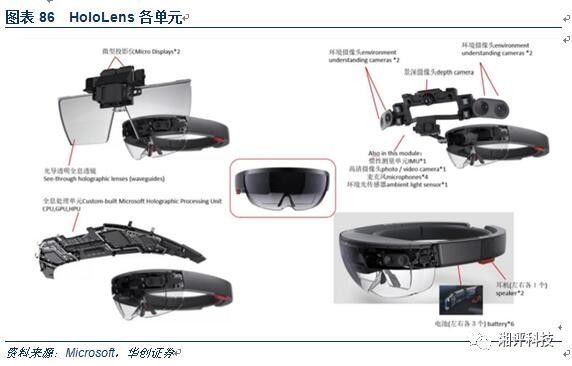
除了3Dæ‘„åƒæ¨¡å—,就是最关键的光å¦æˆåƒæ¨¡å—。目å‰æ¥çœ‹ï¼ŒHoloLensé…备两å—光导é€æ˜Žå…¨æ¯é€é•œï¼Œè™šæ‹Ÿå†…容采用LCoS(硅基液晶)投影技术,从å‰æ–¹å¾®åž‹æŠ•å½±ä»ªæŠ•å°„至光导é€é•œåŽè¿›å…¥äººçœ¼ã€‚
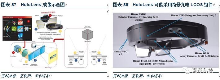
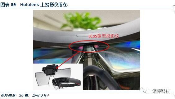
LCOS(液晶覆硅技术)是å°åž‹åŒ–AR头显的关键技术之一。三片å¼çš„LCOSæˆåƒç³»ç»Ÿï¼Œé¦–先将投影光æºå‘出的白色光线,通过分光系统系统分æˆçº¢ç»¿è“三原色的光线,然åŽï¼Œæ¯ä¸€ä¸ªåŽŸè‰²å…‰çº¿ç…§å°„到一å—åå°„å¼çš„LCOS芯片上,系统通过控制LCOSé¢æ¿ä¸Šæ¶²æ™¶åˆ†å的状æ€æ¥æ”¹å˜è¯¥å—芯片æ¯ä¸ªåƒç´ 点å射光线的强弱,最åŽç»è¿‡LCOSå射的光线通过必è¦çš„å…‰å¦æŠ˜å°„汇èšæˆä¸€æŸå…‰çº¿ï¼Œç»è¿‡æŠ•å½±æœºé•œå¤´ç…§å°„到å±å¹•ä¸Šï¼Œå½¢æˆå½©è‰²çš„图åƒã€‚在Hololensä¸ï¼Œé è¿‘é¼»æ¢å¤„的两处å‘光点就是LCoS微型投影仪所在处。目å‰åœ¨æŠ•å½±å…‰æºä¸Šä¸»è¦æœ‰LED和激光两ç§æ–¹æ¡ˆï¼Œç”±äºŽæ¿€å…‰åœ¨å…‰æŸè´¨é‡ã€äº®åº¦ã€åŠŸè€—å’Œä½¿ç”¨å¯¿å‘½ä¸Šæ— å¯æ¯”拟的优越性,我们认为其将是未æ¥çš„å‘展方å‘。
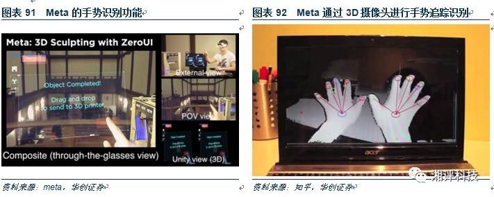
å¦ä¸€æ¬¾ä¸»æµAR产å“MetaåŒæ ·é‡‡ç”¨äº†åŸºäºŽTOFçš„3Dæ‘„åƒå¤´æŠ€æœ¯ä»¥åŠåˆ©ç”¨åŸºäºŽåŠååŠé€é•œçš„投影技术进行æˆåƒã€‚
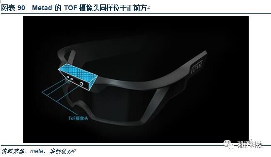
Metaçš„3Dæ‘„åƒå¤´æ¨¡å—由一对高清摄åƒå¤´å’Œä¸€ä¸ªçº¢å¤–探测器组æˆï¼Œåˆ©ç”¨TOF技术获å–图åƒæ·±åº¦ä¿¡æ¯ï¼Œèƒ½å¤Ÿå®žçŽ°åŠ¿è¯†åˆ«ã€QRç (二维ç 的一ç§ï¼‰è·Ÿè¸ªã€ç‰¹å¾è·Ÿè¸ªã€æƒ¯æ€§æµ‹é‡å•å…ƒç‰æ ¸å¿ƒåŠŸèƒ½ã€‚
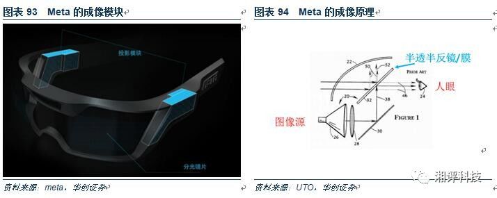
Metaçš„æˆåƒæ–¹å¼åˆ™æ˜¯åŸºäºŽåŠååŠé€é•œçš„æŠ•å½±æŠ€æœ¯ï¼Œé€ åž‹æžå…¶ç´§å‡‘的投影仪è—在镜框内,左å³å„有一个。由LEDå…‰æºå°†åŠé€å¼LCD上的影åƒæŠ•å°„到åŠååŠé€è†œä¸Šï¼Œç„¶åŽå‘射进人眼进行æˆåƒï¼Œä»Žè€Œæ供立体视觉。
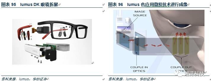
以色列Lumusçš„AR眼镜也采用了微型投影技术,æˆåƒå…³é”®éƒ¨ä»¶ç”±å¾®åž‹æŠ•å½±ä»ªã€å…‰å¯¼å…ƒä»¶ï¼ˆLOE)和å射波导组æˆã€‚æ¤å…¥çœ¼é•œçš„微型投影仪(例如激光投影)将图åƒç”»é¢è¿›è¡ŒæŠ•æ”¾ï¼Œé€šè¿‡å…‰å¯¼å…ƒä»¶ã€å射波导形æˆå…¨å射。
我们认为,微投æˆåƒå’Œ3Dæ‘„åƒæ˜¯æœªæ¥ARäº§ä¸šä¸¤å¤§æ ¸å¿ƒæŠ€æœ¯ï¼Œä»¥VCSEL为代表的åŠå¯¼ä½“激光器件将æˆä¸ºARå…‰å¦æŠ€æœ¯çš„最基础部件,引领消费电åå…‰å¦æ—¶ä»£åˆ°æ¥ï¼
éšç€æŠ•å½±æ˜¾ç¤ºæŠ€æœ¯çš„å‘展,对投影系统的亮度ã€è§£æžåº¦ã€è‰²å½©ä¸°å¯Œæ€§çš„è¦æ±‚将会越æ¥è¶Šé«˜ï¼Œå…‰æºä½œä¸ºæŠ•å½±ç³»ç»Ÿçš„é‡è¦éƒ¨ä»¶ï¼Œå…¶å‘光特性将直接决定投影系统质é‡ã€‚激光光æŸè‰²åº¦ã€ç…§åº¦é«˜åº¦å‡åŒ€ï¼Œå…·æœ‰äº®åº¦é«˜ã€å•è‰²æ€§å¥½ã€æ³¢é•¿å›ºå®šç‰ä¼ 统光æºæ— å¯æ¯”拟的优势,未æ¥å–代LEDæˆä¸ºå¾®åž‹æŠ•å½±æ¨¡å—ã€æŠ•å½±ä»ªã€æŠ•å½±ç”µè§†ç‰è®¾å¤‡å…‰æºå°†æ˜¯å¤§æ¦‚率事件。
ç›®å‰ï¼Œæ¿€å…‰æ˜¾ç¤ºæŠ€æœ¯ä¸»è¦æœ‰ä¸‰åŸºè‰²çº¯æ¿€å…‰ã€è§å…‰ç²‰+è“å…‰ã€LED+激光混åˆå…‰æºä¸‰ç§æŠ€æœ¯ï¼Œå¯¹æ¯”æ¥çœ‹ï¼Œä¸‰åŸºè‰²çº¯æ¿€å…‰ä¼˜åŠ¿è¾ƒä¸ºæ˜Žæ˜¾ã€‚
三基色激光被业界视为最æ£ç»Ÿçš„激光光æºï¼Œå…¶å…·æœ‰è‰²åŸŸå¹¿ã€å…‰æ•ˆé«˜ã€å¯¿å‘½é•¿ã€åŠŸè€—低ã€ä¸€è‡´æ€§å¥½ã€è‰²æ¸©äº®åº¦å¯è°ƒã€ç¨³å®šã€å®‰å…¨å¯é å…维护ã€åº”用çµæ´»ç‰ä¼˜ç‚¹ã€‚三基色光æºç”±å•è‰²å…‰ï¼Œçº¢ã€ç»¿ã€è“三色光分别调制,彩色效果éžå¸¸ç†æƒ³ã€‚
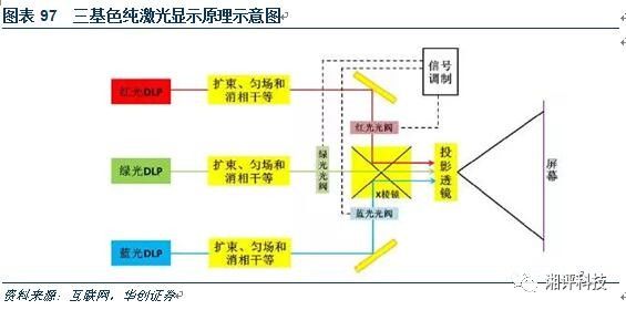
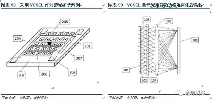
技术进展æ¥çœ‹ï¼Œçº¢å…‰æ¿€å…‰äºŒæžç®¡æŠ€æœ¯ï¼ˆåŒ…括VCSEL红光阵列)å‘展已ç»å分æˆç†Ÿï¼Œè“光激光二æžç®¡ä»·æ ¼å°šé«˜ï¼Œç»¿å…‰æ¿€å…‰äºŒæžç®¡åˆ™è¿˜æœ‰å¾…å‘展。从已披露专利æ¥çœ‹ï¼Œç›®å‰å·²æœ‰â€œçº¢å…‰VCSEL阵列+è“å…‰VCSEL阵列+绿色全固体激光器â€çš„解决方案,VCSELå•å…ƒç”¨äºŽå‘出圆化激光光æŸï¼Œç»è¿‡å¾®é€é•œé˜µåˆ—准直化åŽä½œä¸ºRã€B光输出。æ¤å¤–,采用VCSELé¢é˜µå¯ä»¥å‡å°‘VCSEL激光器之间的干涉性,弱化激光散斑,从而æ高投影显示质é‡ã€‚
è§å…‰ç²‰æ¿€å…‰å³ç›®å‰è¾ƒä¸ºå¸¸è§çš„å•è‰²æ¿€å…‰+DLP技术和å•è‰²æ¿€å…‰+3LCD技术,å•è‰²æ¿€å…‰+DLP技术使用å¯ä»¥æ¿€å‘RGBä¸åŒé¢œè‰²å…‰çš„è§å…‰ç²‰è‰²è½®æ¥å®žçŽ°ï¼Œå•è‰²æ¿€å…‰+3LCD技术则是通过å•è‰²æ¿€å…‰ç…§å°„è§å…‰ç²‰æ¿€
The so-called mini projector is also called pico projector, TRT-Lcos Portable Projector. Mainly through the 3M LCOS RGB three-color projector and 720P film decoding technology, the traditional huge projector is refined, portable, miniaturized, entertaining and practical, making the projection technology closer to life and entertainment.
Usually the projector has certain regulations on 2 aspects:
a). Size: Usually the size is the size of a mobile phone.
b). Battery life: It is required to have at least 1-2 hours or more of battery life when it is not connected to power.
In addition, its general weight will not exceed 0.2Kg, and some do not even need fan cooling or ultra-small silent fan cooling. It can be carried with you (it can be put into your pocket), and the screen can be projected to 40-50 inches or more.
Advantage:
1. Completely replace the MP5 player, video, listening to songs, playing games, e-books, picture browsing, etc. MP5 video is affected by physical performance, the screen can not be bigger, and the screen of this thing is at least 20 inches.
2. Instead of the TV function, the machine can have a built-in CMMB function, or it can be directly connected to the set-top box to play the TV, and it can be used as a 21-inch TV during the day.
Look, it can be used as a 60-100-inch TV at night to achieve the effect of home theater; it is convenient to move and break through the traditional film and television space. Even if you are on the mountain, you can also share today's TV series, movies, and MTV with your lover.
3. Business office: instead of large projectors, it is used for company meetings; the price of large projectors is 4,000 to 14,000, and the lamp life is more than 1,000 hours, which is not convenient to carry. 30,000 hours, no need to change the bulb for 3 years, easy to carry, the salesman only needs to bring a micro projector to demonstrate the new product, which can achieve the demonstration effect.
4. Teaching: training meetings, classroom teaching; traditional projectors are not easy to carry. In school classrooms, due to the naughty students, projectors are not safe to place in the classroom and are easily damaged by students. The portability of micro projectors makes up for the teaching vacancies. In the future, teachers only need to store the materials in the projector and show them to students for teaching, saving the trouble of textbooks and handwriting with pens and chalks.
In addition, the micro-projection has no radiation, which can fully protect pregnant women and people with myopia. Its low power consumption function is 1/1,000,000 of the power consumption of color TVs. One day of electricity has completely impacted the indicators of safety, environmental protection, health, etc., and has made amazing contributions to future social development, standing at the peak of the green world as a leader.
best mini projectors under £100,mini projector pvo portable projector,mini projector portable,mini projector amazon,mini projectors for movies
Shenzhen Happybate Trading Co.,LTD , https://www.happybateprojectors.com