At present, three-dimensional imaging technology has not been maturely applied to surveillance products at home and abroad. The product with similar functions is the vehicle intelligent panoramic surveillance system. However, it can only record plane information and cannot fully reflect the specific conditions of the surrounding environment.
The 360-degree panoramic intelligent monitoring solution introduced to you today is developed from the vehicle intelligent panoramic monitoring system and is an improvement to the vehicle intelligent panoramic monitoring system.
By adopting 3D imaging technology and voice mixing algorithm, the system realizes 3D modeling and scale measurement of surrounding objects on the one hand. On the other hand, it also records all the sound information of all observation points, making the recorded data more vivid, vivid and comprehensive.
This system scheme can be widely used in all-round intelligent monitoring of important occasions such as medium and high-end automobiles, construction machinery, port locks, reservoirs and dams, and financial places.
System basic principle description
The three-dimensional intelligent panoramic monitoring system is mainly divided into the following parts: central processing unit, display and man-machine interface, special camera (distributed installation).
The main body of this system is the central processing unit, which mainly includes:
(1) Video capture component, capture the video required by the system, and transmit the captured video to the video synthesis component.
(2) Video anti-shake components, to the greatest extent possible to prevent jitter in the video capture process, while performing corresponding video compensation operations.
(3) Video synthesis component, seamlessly synthesize the collected video content to form a panoramic video, and send it to the projection and mapping unit.
(4) Projection and mapping component, which projects and maps the synthesized video content and outputs it to the corresponding terminal.
(5) Target detection component, intelligent detection of surrounding target objects, intelligent control operation, comprehensive obstacle warning and multiple navigation information according to preset rules.
(6) GIS components, GIS positioning function for mobile subjects.
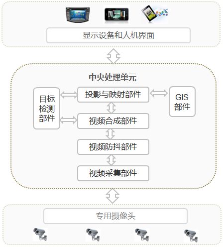
Figure 1 Framework diagram of the system scheme
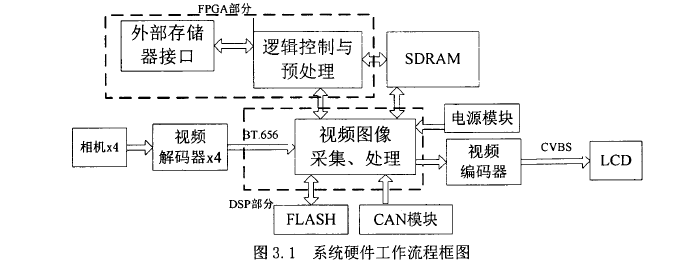
System hardware workflow diagram
The system scheme mainly includes: DSP core processor unit, FPGA co-processor unit, image acquisition unit (camera), video decoding chip, video encoding chip, CAN module. Figure 3.1 The working flow diagram of the system hardware.
Selection, discussion and analysis of the main components of the system hardware platform
The hardware platform device selection of this system is analyzed based on the optimization of various performance indicators such as system stability, scalability and future software upgrade space. Each device is also selected on the basis of reducing the system cost as much as possible and making full use of the internal resources of each chip to improve the integration and cost performance of the entire system.
(1) TMS320C6000 series DSP analysis
In this design, DSP is regarded as the core processing device, its selection determines the complexity of the peripheral circuit and the stability of the whole system. In order to achieve the special requirements of the panoramic parking assistance system with multi-image sensor fusion, the selection of the core processor DSP determines the structure of the entire system circuit.
DM642 retains the original core structure of C64x and most of its peripherals, and adds 3 dual-channel digital video seamless interfaces for applications such as multi-channel video capture processing, which can capture up to 6 digital video streams at the same time. Its on-chip resources are rich and expansibility is good, it is most suitable for the requirements of this design, after comprehensive consideration, finally choose DM642 as the core processor of this design.
Choose DM642 as the core processor of this design, the overall functional block diagram of DM642 is shown as in Fig. 3.2.
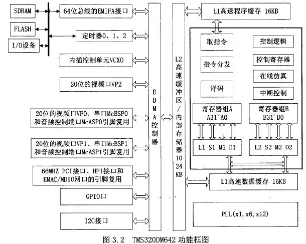
DM642 uses L1P and L1D two-level cache structure inside, with powerful and rich peripheral equipment interfaces. L1P and L1D are the first level program cache and the second level data cache respectively. LIP is a directly mapped cache space, and L1D is a two groups of connected high-speed data cache space n 2|.
Peripheral equipment includes: 3 configurable video ports, 1 Ethernet controller module, 1 high-speed data input/output management module, 1 plug-in VCXO control interface, 1 multi-link dedicated audio interface, 1 12C bus Hardware standard interface, 2 configurable multi-channel buffer serial ports, 3 configurable 32-bit timers, 1 expansion interface (PCI) with peripheral equipment, 1 group of 16-pin configurable I/O ports (GPIO), A 64-bit IMIFA can seamlessly connect synchronous/asynchronous memory and peripheral expansion devices.
(2) Selection and analysis of FPGA
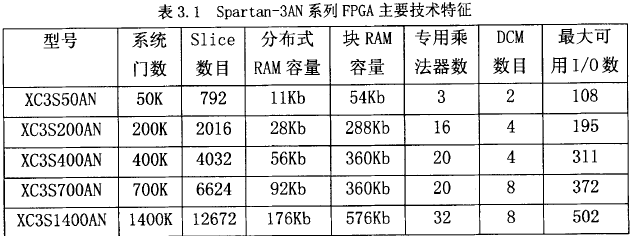
After investigation, this design finally selected the Spartan-3AN series XC3S400AN chip with 400,000 system gates, so it focuses on the resource peripherals and other related information n6 of this chip.
The Spartan-3AN series of chips are non-volatile FPGAs with very high system integration. This chip has the following unique features: FPGA has a large amount of internal SRAM high-performance resources, non-volatile, reduced board space and convenient configuration, etc. Features.
Spartan-3AN. The hardware platform is specially developed for embedded products that have strict cost requirements.
The hardware resources of Spartan-3AN series FPGA chip are shown in Table 3.1.
(3) Selection and analysis of image sensor
Image sensors include electron beam camera tubes, CCD, CMOS and other ultra-large-scale semiconductor integrated image sensors and area array high-speed scanning image sensors. The internal structure block diagram of CMOS image sensor is shown as in Fig. 3.3.
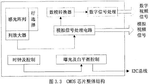
In the course of the development of CMOS devices, the evolution of CMOS devices from "passive image sensitive unit" structure to "active image sensitive unit" is due to the large-scale integrated circuit design and microelectronics manufacturing technology entering the deep sub-micron stage, and CMOS image sensor chips can be integrated The large-scale photosensitive array, signal readout and processing circuit, and control circuit are integrated, together with optical lenses and other peripheral equipment to form an optical imaging system.
The internal structure of CMOS chips under modern technological conditions is mainly composed of photosensitive arrays, horizontal (vertical) control circuits and sequential circuits, signal readout and processing circuits, analog/digital conversion circuits and data interface circuits.
The following two image sensors are analyzed, namely, MT9V024 and 0v7960 image sensor chips of different companies.
(1) MT9V024 image sensor
MT9V024 is a CMOS active pixel image sensor with an image plane size of 1/3 inch and wide VGA mode. It uses TrueSNAP spherical shutter and high dynamic range. The sensor is specially designed for the needs of automotive imaging both inside and outside, which makes it an ideal chip for a variety of imaging applications.
This sensor uses Aptina's breakthrough low-noise CMOS imaging technology to achieve CCD imaging quality (based on signal-to-noise ratio and low-light sensitivity) while maintaining the inherent size, cost, and CMOS integration advantages.
Advanced camera functions such as 2×2 and 4×4 are used on the chip to improve the sensitivity when operating at smaller resolutions, just like window functions, row and column mirroring. Through the standard two-wire serial programmable interface, the frame size, exposure, gain and other parameters can be configured in the default mode. The default mode outputs a wide VGA size image at 60 frames per second.
The on-chip analog-to-digital converter converts the analog signal of each pixel into a ±Obit data stream. Can additionally enable a 12-bit full resolution instead of 10-bit small signal. In addition to the traditional parallel logic output, MT9V024 also has a LVDS (serial low voltage differential signal) sensor that can operate in stereo cameras. The specific performance parameters of the MT9V024 image sensor are shown in Table 3.2:

(2) 0V7960 image sensor
0V7960 is a small-size image sensor chip newly launched by OMNIVISION in the last two years. Its appearance meets the requirements of the automotive industry for assisted driving system applications (such as rearview mirrors), and creates a new application of CMOS image sensors in automotive safety assisted driving systems. The performance of the 0V7960 image sensor fully meets the special needs of the automotive electronics industry for the imaging effect of the image sensor. It is 1/4 ultra-small and has good performance in low light (
The specific performance parameters of the 0V7960 image sensor are shown in Table 3.3:
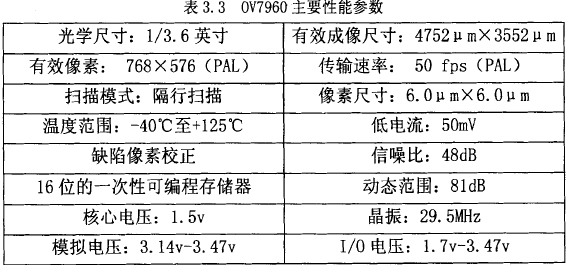
The purpose of this design is to develop a panoramic parking assist system that can break the existing panoramic parking assist system that is only equipped on high-end cars. Therefore, low cost is one of the factors that must be considered in system development. Since the system used for automotive active safety provides the driver with real-time information about the surrounding conditions of the vehicle, the system does not require particularly high image quality. After comprehensive consideration, the design Only use 0V7960 image sensor as the camera's image acquisition chip.
Power circuit design
Since this system contains DSP, FPGA and their peripheral circuit devices, the required power supply includes 5v, 3.3v, 2.5v, 1.8v, 1.4v, 1.2v, etc., the system requires so many power modules The design will become the difficulty of the whole system, whether it can ensure the stable operation of each part of the system becomes the key to the success or failure of the whole hardware design. The power supply of each module device will be explained below.
1. DSP and peripheral equipment power supply circuit
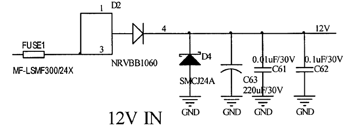
When the car is started and during normal driving, the output voltage of its power supply changes irregularly in the range of lOV-16V. It is not difficult to imagine the harm of such a large fluctuation voltage to the electronic system. If it is directly applied to the on-board electronic system and on-board instrumentation, the voltage shock generated by this large fluctuation will often cause damage to the electronic devices and cause serious accidents.
Therefore, in the design of this system, when the 12V power supply is to be introduced from the car, a protection circuit is added to ensure the safety of the entire system circuit, as shown in Figure 3.4:
Figure 3.4 12V protection circuit
In order to ensure the stable operation of the TMS320DM642 processor, its core and I/O ports must be independently powered to reduce crosstalk between the power supplies. The core voltage is 1.4V, and the I/O port power supply is 3.3V. Video coding chip TVP5150AMl digital voltage (AVDD) and analog voltage (DVDD) input are 1.8 V, and the I/O terminal IZl voltage (DVDDIO) is 3.3 V.
The video coding chip SAATl21 digital voltage (VDDD) and analog voltage (VDDA) are the same as 3.3V. The working voltage of GDRAM and FLASH is 3.3V. Considering the power consumption of the entire system, the first-level voltage conversion selects TI's recommended switching power management chip TPS5430 as the 12V-5V voltage conversion core device; selects two TPS54310 to design the circuit with reference to its DataSheet, and provide the core for the DSP. The voltage is 1.4V and the I/O port voltage is 3.3V, of which the 3.3V power supply also supplies power for other components in the system. The circuit design of each part is as follows:
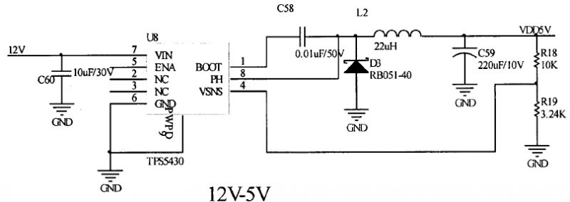
Figure 3. 5 TPS5430 power conversion circuit 12V-5V
The input voltage of TPS54310 is the 5V voltage output by TPS5430 after conversion. One piece of TPS54310 is
TMS320DM642 provides the core voltage, the output voltage is 1.4V as shown in circuit diagram 3.9, and the other one provides I/O port voltage for TMS320DM642, and the output voltage is 3.3V as shown in Figure 3.6:
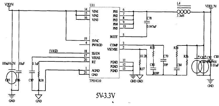
Figure 3.6 DM642 peripheral I/0 port voltage
After the system is powered on, the DSP core first obtains the 1.4V stable voltage provided by the TPS54310 power chip, and then the PV/RGD port of the first TPS54310 outputs an enable level (high level) to the SS/ of the second TPS54310 EN port old cited. This guarantees that the DSP core gets the power supply first when the system is powered on, and the IlO port gets 3.3V power supply after the core gets a stable voltage of 1.4V. The DSP core loses power at the i/o port during the system power down process. This greatly increases the service life of the chip and system stability.
2. FPGA and other part of the power module design
What FPGA coprocessor chooses is Xilinx Spartan-3AN series chip, its model is XC3S400AN. The core voltage (VCCINT) of the XC3S400AN processor is 1.2V, the auxiliary power supply voltage (VCCAUX) is 2.5V, and the i/o port voltage is 3.3V.
Other chips on the board, such as FPGA configuration chip XCF02SV020C power supply is 2.5V and 3.3V, TVP5150AMl voltage (AVDD, DVDD) is 1.8V and I/O port voltage (DVDDIO) is 3.3V, SAA7121 voltage is 3. .3V.
Since the power input 12V is converted by the first-level switching power supply such as TPS54310 and TPS5430, the subsequent voltage conversion chips are all linear power conversion chips with simple design and small space occupation, such as TLVll17-1.2 for the FPGA core. 2V stable voltage, TLVlll7-1. 8 provides 1. 8v digital voltage for TVP5150AMl, and TLVll17-2.5 is FPGA's auxiliary power supply and configuration chip power supply. The circuit design is shown in Figure 3.7 below
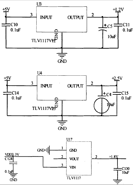
Figure 3. 7 FPGA and other power modules
Camera design based on 0V7960 image sensor
The circuit design of the core part of the 0V7960 image sensor is briefly introduced below. Whether the camera can output a stable analog signal correctly is the key to the design of the camera part. A power chip with a small output voltage ripple coefficient and a large number of filter capacitors must be used. The filter capacitor should be placed as close to the pin as possible, so that a good simulation can be output. Video image data. The image sensor design circuit is shown in Figure 3. 8:
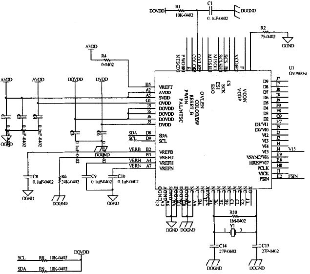
Figure 3. 8 0V70960 image sensor peripheral circuit
Practical application of three-dimensional intelligent panoramic monitoring system
This system has been practiced and applied on the vehicle's three-dimensional panoramic monitoring system. The panoramic view effect of the effective area in the monitoring range virtualized by the video synthesis by this system, and displayed in the form of three-dimensional images, provides a more realistic virtual scene. At the same time, the system can also realize automatic scale measurement of key parts, and actively alarm when necessary. The effect demonstration diagram is as follows:
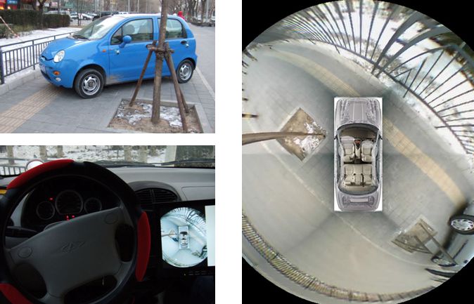
Figure 3 Application effect diagram of 3D intelligent panoramic monitoring system in vehicle monitoring
Dongguan Guancheng Precision Plastic Manufacturing Co., Ltd. , https://www.dpowergo.com